Introduction to Copper-Soldermask Comparison
In the world of printed circuit board (PCB) manufacturing, the choice between copper defined and soldermask defined pads can significantly impact the overall performance, reliability, and manufacturability of the board. This article will delve into the advantages and disadvantages of each approach, helping designers and manufacturers make informed decisions based on their specific requirements.
What are Copper Defined Pads?
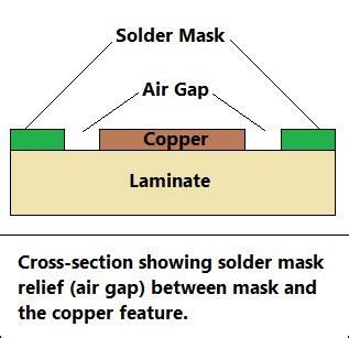
Copper defined pads are a design approach where the copper layer of the PCB determines the size and shape of the pads. In this method, the soldermask opening is slightly larger than the copper pad, exposing the entire copper surface for soldering.
What are Soldermask Defined Pads?
Soldermask defined pads, on the other hand, rely on the soldermask layer to define the size and shape of the pads. The copper pad is made larger than the desired soldermask opening, and the soldermask layer is used to create the final pad dimensions.
Advantages of Copper Defined Pads
1. Better Copper Etching Control
One of the primary advantages of using copper defined pads is the increased control over the copper etching process. Since the copper layer directly determines the pad size and shape, manufacturers can achieve more precise and consistent results.
2. Improved Solderability
Copper defined pads offer better solderability compared to soldermask defined pads. With the entire copper surface exposed, the solder can form a stronger bond with the pad, resulting in a more reliable solder joint.
3. Reduced Soldermask Misalignment Issues
Using copper defined pads minimizes the risk of soldermask misalignment issues. Since the soldermask opening is larger than the copper pad, slight misalignments during the soldermask application process will not affect the final pad dimensions.

Disadvantages of Copper Defined Pads
1. Increased Risk of Solder Bridging
One potential drawback of copper defined pads is the increased risk of solder bridging, especially in designs with closely spaced pads. The exposed copper surface between pads can allow solder to flow and create unintended connections.
2. Limited Pad Size Reduction
Copper defined pads may limit the ability to reduce pad sizes in high-density designs. As the copper layer determines the pad dimensions, reducing the pad size requires modifying the copper artwork, which can be more challenging than adjusting the soldermask openings.

Advantages of Soldermask Defined Pads
1. Better Control Over Solder Paste Volume
Soldermask defined pads provide better control over the solder paste volume applied to the pads. The soldermask opening determines the area where solder paste can be deposited, allowing for more precise control and reducing the risk of excessive solder application.
2. Reduced Risk of Solder Bridging
By using soldermask to define the pad dimensions, designers can reduce the risk of solder bridging between closely spaced pads. The soldermask layer acts as a barrier, preventing solder from flowing beyond the desired pad area.
3. Easier Pad Size Reduction
Soldermask defined pads offer more flexibility when it comes to reducing pad sizes in high-density designs. Since the pad dimensions are determined by the soldermask openings, designers can easily adjust the pad size without modifying the copper artwork.

Disadvantages of Soldermask Defined Pads
1. Potential Soldermask Misalignment
One of the main disadvantages of soldermask defined pads is the potential for soldermask misalignment. If the soldermask layer is not precisely aligned with the copper pads, it can result in inconsistent pad sizes and shapes, affecting solderability and component placement accuracy.
2. Reduced Solderability
Soldermask defined pads may have reduced solderability compared to copper defined pads. Since a portion of the copper pad is covered by the soldermask, the available surface area for solder bonding is reduced, potentially leading to weaker solder joints.
Comparison Table
| Feature | Copper Defined Pads | Soldermask Defined Pads |
|---|---|---|
| Copper Etching Control | Better | Good |
| Solderability | Excellent | Good |
| Soldermask Misalignment Risk | Low | High |
| Solder Bridging Risk | High | Low |
| Pad Size Reduction Flexibility | Limited | Excellent |
| Solder Paste Volume Control | Good | Excellent |
Frequently Asked Questions (FAQ)
1. When should I use copper defined pads?
Copper defined pads are ideal when precise control over the copper etching process is required, and solderability is a top priority. They are also suitable for designs with larger pad sizes and spacing, where the risk of solder bridging is minimal.
2. When should I use soldermask defined pads?
Soldermask defined pads are recommended for high-density designs with closely spaced pads, as they reduce the risk of solder bridging. They also provide better control over solder paste volume and offer more flexibility in reducing pad sizes.
3. Can I use a combination of copper defined and soldermask defined pads in the same design?
Yes, it is possible to use a combination of both pad types in the same design. Designers can choose the appropriate approach for different components or areas of the PCB based on their specific requirements.
4. How do I minimize soldermask misalignment issues?
To minimize soldermask misalignment issues, ensure that your design files are accurately created and adhere to the manufacturer’s guidelines. Communicate closely with your PCB manufacturer and discuss their soldermask alignment capabilities and tolerances.
5. What other factors should I consider when choosing between copper defined and soldermask defined pads?
Other factors to consider include the PCB manufacturing process capabilities, component specifications, and the intended application environment. Consult with your PCB manufacturer and component suppliers to determine the best approach for your specific project.
Conclusion
Choosing between copper defined and soldermask defined pads is an important decision in PCB design and manufacturing. Both approaches have their advantages and disadvantages, and the ultimate choice depends on factors such as design requirements, component specifications, and manufacturing process capabilities.
By understanding the strengths and limitations of each approach, designers and manufacturers can make informed decisions that optimize the performance, reliability, and manufacturability of their PCBs. Effective communication and collaboration between design teams and PCB manufacturers are essential to ensure the successful implementation of the chosen pad definition method.


Leave a Reply