An In-Depth Look at the Benefits and Challenges of Additive PCB Fabrication
The world of printed circuit board (PCB) manufacturing is rapidly changing. While subtractive methods have long dominated the industry, additive fabrication techniques are quickly emerging as a promising alternative. Additive PCB manufacturing, also known as additive PCB printing, offers a range of potential benefits over traditional subtractive techniques. In this article, we’ll take an in-depth look at additive PCB fabrication – what it is, why it matters, key benefits and challenges, and what the future may hold for this nascent manufacturing approach.
What is Additive PCB Manufacturing?
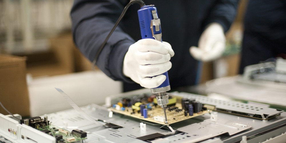
Additive PCB manufacturing utilizes a layer-by-layer build-up process to create circuit boards, rather than the removal of material used in subtractive techniques. The most common additive technologies used today include:
- Aerosol jet printing – uses an aerodynamic focusing technique to deposit inks as tiny droplets.
- Inkjet printing – similar to desktop 2D inkjet printers but with specialty inks and 3D capabilities.
- 3D Printing – fused filament fabrication (FFF), stereolithography (SLA), and other 3D printing methods can construct PCBs from the ground up.
- Plating – electrolytic and electroless plating methods allow layered metal deposition onto substrates.
These additive processes build up PCBs layer-by-layer directly from CAD data. This contrasts with the traditional approach of starting with a blank substrate and using milling, etching, drilling and other techniques to remove material. The additive approach minimizes waste and offers new possibilities for optimized designs.
Why Additive PCB Manufacturing Matters
There are several key reasons why additive PCB fabrication methods are generating so much interest:
- Design Freedom – By working directly from CAD models, additive can fabricate designs not feasible with subtractive techniques. This includes complex 3D structures, embedded components, and flexible substrates.
- Customization – Printed electronics enable cost-effective short-run and one-off productions. Lead times can be reduced from weeks to days.
- Simplified Process – Additive methods skip many time-consuming fabrication steps like masking, etching, stripping and drilling. Steps are consolidated and automation enhanced.
- Less Waste – Subtractive processes material removal results in significant waste. Additive only deposits required material minimizing waste streams.
- Lightweighting – Organic shapes and lattice structures facilitate weight reductions in end products. This is attractive for portable electronics and aerospace applications.
Many experts see additive PCB fabrication as an enabling technology for the electronics industry. As processes mature, productivity improves and costs drop – wider adoption seems inevitable.
Benefits and Advantages of Additive PCB Manufacturing
Additive PCB fabrication offers a number of benefits and advantages compared to traditional subtractive techniques:
Faster Turnaround Times
The simplified processes and digital workflow intrinsic to additive manufacturing enable much faster production times. Design to production can readily be achieved in 1-2 days versus 4-6 weeks for conventional methods. This facilitates rapid prototyping and market responsiveness.
Design Freedom
Additive processes offer almost unlimited design freedom compared to subtractive methods. 3D structures, embedded components, flexible substrates and other advances are possible. This expanded design envelope enables performance improvements and product innovations.
Reduced Costs for Low Volume
While additive methods remain cost prohibitive at higher volumes, they offer clear cost advantages for short runs and prototypes. By eliminating tooling and simplifying processes, raw board costs can be 80% less for volumes under 1,000 units.
Less Material Waste
Because additive only deposits required materials precisely, it generates far less waste than the material removal of subtractive machining. This reduces materials costs and disposal fees. It also supports environmental goals around waste and resource reduction.
Rapid Changes and Redesigns
With additive methods, design changes can be implemented almost immediately with little added time or cost. This facilitates design optimization and accommodates late-stage client changes. Subtractive processes rely on fixed tooling inhibiting quick changes.
Simplified Supply Chains
Printing circuit boards on demand locally reduces logistics costs, lead times and inventory needs. Reliance on offshore fabrication and complex global supply chains is reduced. This also helps mitigate geopolitical supply chain risks.
Challenges Facing Additive PCB Manufacturing
While holding great promise, additive PCB fabrication does face some challenges and barriers to broader adoption:
Quality and Reliability
Many additive processes remain a work in progress when it comes to matching the quality and reliability achieved with mature subtractive methods. Factors like resolution, component adhesion, layer registration and material performance still require refinement.
Limited Scalability
All additive processes have limitations around maximum part sizes they can accommodate. Most remain suited for small, prototype or medium volume runs. Expanding build envelopes and raising throughput for higher volumes is still required.
Material Limitations
The material selection for additive electronics remains narrower than subtractive processes. Thermoplastics and other materials have presented challenges for printing, limiting options. Expanded certified material choices are critical for wider adoption.
Process Control and Standards
Quality control procedures and manufacturing standards for additive PCB remain in development. Quantifying reliability requires extensive testing. Lack of standards inhibits quality guarantees needed for production situations.
Cost for Medium/High Volumes
While additive techniques are cost effective at lower volumes, they remain prohibitively expensive for larger production runs. Expanding production scale and optimizing processes is necessary to be cost competitive with etching.
The Future of Additive PCB Fabrication
While additive PCB manufacturing faces obstacles, rapid innovation in the field points to a bright future. Here are some exciting developments on the horizon:
Hybrid Additive/Subtractive Platforms
Combining additive and subtractive in one system capitalizes on their respective strengths – additive flexibility and subtractive speed/accuracy. Hybrid platforms will help accelerate adoption.
High-Volume Production Systems
Leveraging automation and process improvements, full additive production systems suited to higher volumes are under development. This is critical to compete with mature etching.
Advanced Multi-Material Printing
New systems combining micro-dispensing, aerosol jetting and other technologies enable blended prints using conductors, encapsulants and other materials.
Quality and Reliability Testing
Extensive testing to benchmark and validate additive processes will develop missing industry standards and qualifications needed for end-product applications.
Direct Component Integration
Innovations around inline component placement will eliminate secondary assembly steps enabling true print-and-play PCB production.
Many industry experts see additive reaching cost parity with subtractive etching in 5-10 years for an increasing number of applications. This mirrors the trajectory seen in industries like aerospace and automotive, where additive techniques are already entering mainstream manufacturing. With so much active research and financial investment underway, the promise of additive electronics seems less question of if than when.
Frequently Asked Questions
Here are answers to some common questions about additive PCB manufacturing:
What are the resolution limitations of current additive PCB processes?
Most additive systems can presently print features down to around 50-100 microns, with some research demonstrating resolutions below 10 microns. This remains coarser than photolithographic subtractive techniques capable of 5-10 micron geometries. Resolution continues to be a key area of improvement.
What materials can be used in additive PCB fabrication?
Materials used include conductive inks and pastes based on silver, copper or carbon. Dielectric materials include various resins, epoxies and thermoplastics. Material choice remains limited relative to subtractive, with ongoing R&D around high-performance printable materials.
Is surface-mount component integration possible with additive PCBs?
Yes, the latest additive systems provide solutions for integrated component placement. Methods include pick-and-place, dispensed solder jetting and stamping techniques. This enables true print-and-play production, eliminating secondary assembly steps.
Does additive PCB fabrication produce any emissions or hazardous waste?
Additive techniques generate almost no hazardous waste compared to the harsh etchants, stripping chemicals and waste streams of subtractive methods. Most additive platforms run very cleanly with no harmful byproducts. This makes additive processes inherently more environmentally friendly.
What types of products are currently manufactured with additive PCBs?
Additive is currently used mostly for prototypes, small runs and low-volume end products. Applications include consumer electronics, industrial sensors, defense, aerospace, and automotive projects. As the technology matures, uses will expand across nearly all PCB-intensive fields.
Conclusion
Additive PCB manufacturing is an extremely promising technology creating new possibilities in electronics design and production. As processes continue to advance, additive techniques are poised to transform electronics fabrication. Challenges certainly remain, but rapid innovation points to additive methods complementing and in some applications displacing subtractive PCB manufacturing in the not-too-distant future. With its ability to shorten timelines, reduce costs and enable novel designs, additive fabrication seems primed to open exciting new horizons in the world of printed circuit boards.


Leave a Reply