Introduction to Tenting Via in PCB Manufacturing
Tenting via is an important process in the fabrication of printed circuit boards (PCBs). It involves covering the via holes on a PCB with a layer of solder mask material. Vias are small holes drilled through a PCB to electrically connect different layers of the board. Tenting these vias with solder mask helps protect them and improves the reliability and manufacturability of the PCB.
In this comprehensive article, we will delve into the details of tenting via, its importance in PCB fabrication, the different methods used for tenting vias, and frequently asked questions about this critical process.
What are Vias in PCBs?
Before we discuss tenting via, let’s first understand what vias are in the context of PCBs. Vias are small holes drilled through a PCB to create electrical connections between different layers of the board. They allow signals and power to be routed from one layer to another, enabling more complex circuit designs and higher component density on the PCB.
There are several types of vias used in PCB design:
- Through-hole vias: These vias go through all layers of the PCB, from the top to the bottom.
- Blind vias: These vias connect an outer layer to an inner layer, but do not go through the entire board.
- Buried vias: These vias connect inner layers without reaching the outer layers of the PCB.
- Micro vias: These are very small vias, typically less than 0.15mm in diameter, used for high-density interconnect (HDI) PCB designs.
Vias are essential for creating multi-layer PCBs and enabling efficient routing of signals and power across the board. However, exposed vias can be susceptible to contamination, oxidation, and mechanical damage, which is where tenting via comes into play.

What is Tenting Via?
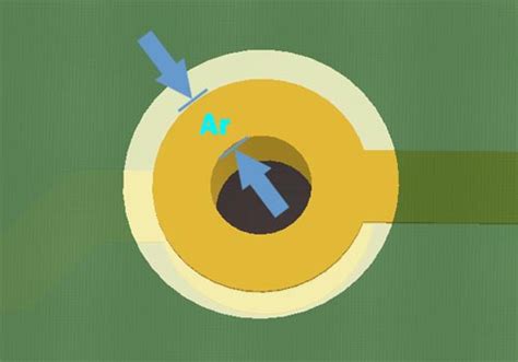
Tenting via is the process of covering via holes with a layer of solder mask material during PCB fabrication. The solder mask is a thin, protective coating applied to the copper traces and pads on a PCB. It serves several purposes, including insulating the copper features, protecting them from oxidation and contamination, and providing a surface for applying solder paste and components.
When a via is tented, the solder mask material covers the entire via hole, creating a smooth, uninterrupted surface on the PCB. This process helps to:
- Protect the via from contamination and oxidation
- Prevent solder from flowing into the via during the soldering process
- Improve the mechanical strength and reliability of the via
- Enhance the cosmetic appearance of the PCB
Tenting via is particularly important for vias that are not used for component assembly, such as those used for routing signals between layers. By covering these vias with solder mask, the PCB becomes more robust and less susceptible to damage during handling and assembly.

Methods for Tenting Vias
There are two primary methods for tenting vias in PCB fabrication:
- Liquid Photo Imageable (LPI) Solder Mask Tenting: This is the most common method for tenting vias. In this process, a liquid photoimageable solder mask is applied to the PCB surface, covering the vias and copper features. The solder mask is then exposed to UV light through a photomask, which hardens the mask in the desired areas. The unexposed areas are then removed using a developer solution, leaving the vias and copper features covered with solder mask.
- Dry Film Solder Mask Tenting: This method involves laminating a dry film solder mask onto the PCB surface. The dry film is a solid, photosensitive material that is applied using heat and pressure. Once laminated, the dry film is exposed to UV light through a photomask, hardening the desired areas. The unexposed areas are then removed using a developer solution, similar to the LPI process.
Both methods have their advantages and disadvantages, and the choice between them depends on factors such as the PCB design, the desired solder mask thickness, and the manufacturing capabilities of the PCB fabricator.

Advantages of Tenting Via
Tenting via offers several key benefits in PCB fabrication:
- Protection from contamination: By covering the via holes with solder mask, tenting via prevents contamination from entering the vias during handling, storage, and assembly. This helps maintain the integrity of the electrical connections and improves the reliability of the PCB.
- Prevention of solder wicking: During the soldering process, molten solder can flow into exposed via holes, causing solder wicking. This can lead to insufficient solder on the component pads, resulting in poor solder joints and potential reliability issues. Tenting via prevents solder from flowing into the vias, ensuring a proper solder joint formation.
- Improved mechanical strength: Tenting via provides additional mechanical support to the via structure, making it more resistant to stress and vibration. This is particularly important for vias in high-stress areas of the PCB, such as near connectors or in applications subject to mechanical shocks.
- Enhanced electrical insulation: The solder mask material used for tenting via acts as an insulator, providing additional electrical insulation between the via and the surrounding copper features. This helps prevent short circuits and improves the overall electrical performance of the PCB.
- Better aesthetics: Tenting via creates a clean, uniform appearance on the PCB surface, as the solder mask covers the via holes and blends seamlessly with the surrounding area. This can be important for applications where the visual appeal of the PCB is a consideration, such as in consumer electronics.
Challenges and Considerations in Tenting Via
While tenting via offers numerous benefits, there are also some challenges and considerations to keep in mind:
- Via size and aspect ratio: Tenting via becomes more challenging as the via size decreases and the aspect ratio (the ratio of via depth to diameter) increases. Smaller vias and higher aspect ratios can make it difficult for the solder mask to fully cover the via hole, leading to incomplete tenting and potential reliability issues.
- Solder mask thickness: The thickness of the solder mask material used for tenting via can impact the effectiveness of the process. If the solder mask is too thin, it may not provide sufficient coverage and protection for the via. On the other hand, if the solder mask is too thick, it can cause issues with solder paste application and component placement during assembly.
- Thermal management: Tenting via can affect the thermal management of the PCB, as the solder mask material has a lower thermal conductivity than the copper used for the vias. This can be a concern for high-power applications or designs with thermal vias used for heat dissipation. In such cases, selective tenting or alternative thermal management strategies may be necessary.
- Cost and manufacturing time: Tenting via adds an additional step to the PCB fabrication process, which can increase the overall cost and manufacturing time. This is especially true for designs with a large number of vias or complex via patterns that require specialized solder mask application techniques.
Best Practices for Tenting Via Design
To ensure the effectiveness and reliability of tented vias, consider the following best practices in your PCB design:
- Follow manufacturer guidelines: Consult with your PCB fabricator and solder mask supplier for their recommended guidelines on via size, aspect ratio, and solder mask thickness for effective tenting via. Adhering to these guidelines will help ensure the best results and minimize potential issues.
- Use appropriate via sizes: When designing vias for tenting, use via sizes that are compatible with the solder mask application process. Avoid using vias that are too small or have high aspect ratios, as these can be difficult to tent effectively.
- Consider selective tenting: In some cases, it may be beneficial to selectively tent vias, leaving some vias exposed for thermal management or other purposes. Work with your PCB fabricator to determine the feasibility and cost implications of selective tenting for your design.
- Optimize via placement: When placing vias on your PCB, consider their location relative to other components and features. Avoid placing vias too close to component pads or in areas where solder mask coverage may be compromised, such as near board edges or tight corners.
- Perform thorough testing: Before finalizing your PCB design, perform thorough testing and validation of the tented vias. This may include visual inspection, electrical testing, and environmental stress testing to ensure the reliability and performance of the tented vias under various conditions.
Frequently Asked Questions (FAQ)
- Q: Can all types of vias be tented?
A: In general, most types of vias can be tented, including through-hole, blind, and buried vias. However, the effectiveness of tenting via depends on factors such as via size, aspect ratio, and the solder mask application process used. - Q: Is tenting via always necessary?
A: Tenting via is not always necessary, but it is highly recommended for vias that are not used for component assembly. Tenting via helps protect the vias from contamination, prevents solder wicking, and improves the mechanical and electrical reliability of the PCB. - Q: Can tenting via affect signal integrity?
A: Tenting via can have a minor impact on signal integrity, as the solder mask material has a slightly different dielectric constant than the PCB substrate. However, for most applications, this impact is negligible and can be mitigated through proper PCB design and material selection. - Q: How does tenting via impact the cost of PCB fabrication?
A: Tenting via adds an additional step to the PCB fabrication process, which can increase the overall cost and manufacturing time. The cost impact depends on factors such as the number of vias, the complexity of the via pattern, and the solder mask application method used. - Q: Can tented vias be repaired if damaged?
A: Repairing tented vias can be challenging, as it involves removing the damaged solder mask material and reapplying it to the affected area. In some cases, localized repairs may be possible using specialized techniques, such as laser or mechanical removal of the damaged solder mask. However, the effectiveness and reliability of such repairs depend on the extent of the damage and the skill of the repair technician.
Conclusion
Tenting via is a critical process in PCB fabrication that involves covering via holes with a layer of solder mask material. This process helps protect the vias from contamination, prevents solder wicking, improves mechanical strength, enhances electrical insulation, and provides better aesthetics for the PCB.
When designing PCBs with tented vias, it is essential to consider factors such as via size, aspect ratio, solder mask thickness, and thermal management. Following best practices and working closely with your PCB fabricator can help ensure the effectiveness and reliability of tented vias in your PCB design.
As PCB technology continues to advance, with increasing component density and more complex designs, the importance of tenting via will only grow. By understanding the benefits, challenges, and best practices associated with tenting via, PCB designers and manufacturers can create more reliable, high-performance PCBs that meet the demands of today’s electronic applications.
| Aspect | Consideration |
|---|---|
| Via Size | Smaller vias are more challenging to tent effectively |
| Aspect Ratio | Higher aspect ratios can make tenting more difficult |
| Solder Mask Thickness | Too thin or too thick can cause issues with tenting |
| Thermal Management | Tenting can affect thermal conductivity, consider alternatives |
| Cost and Manufacturing | Tenting adds an additional step, increasing cost and time |


Leave a Reply