Introduction
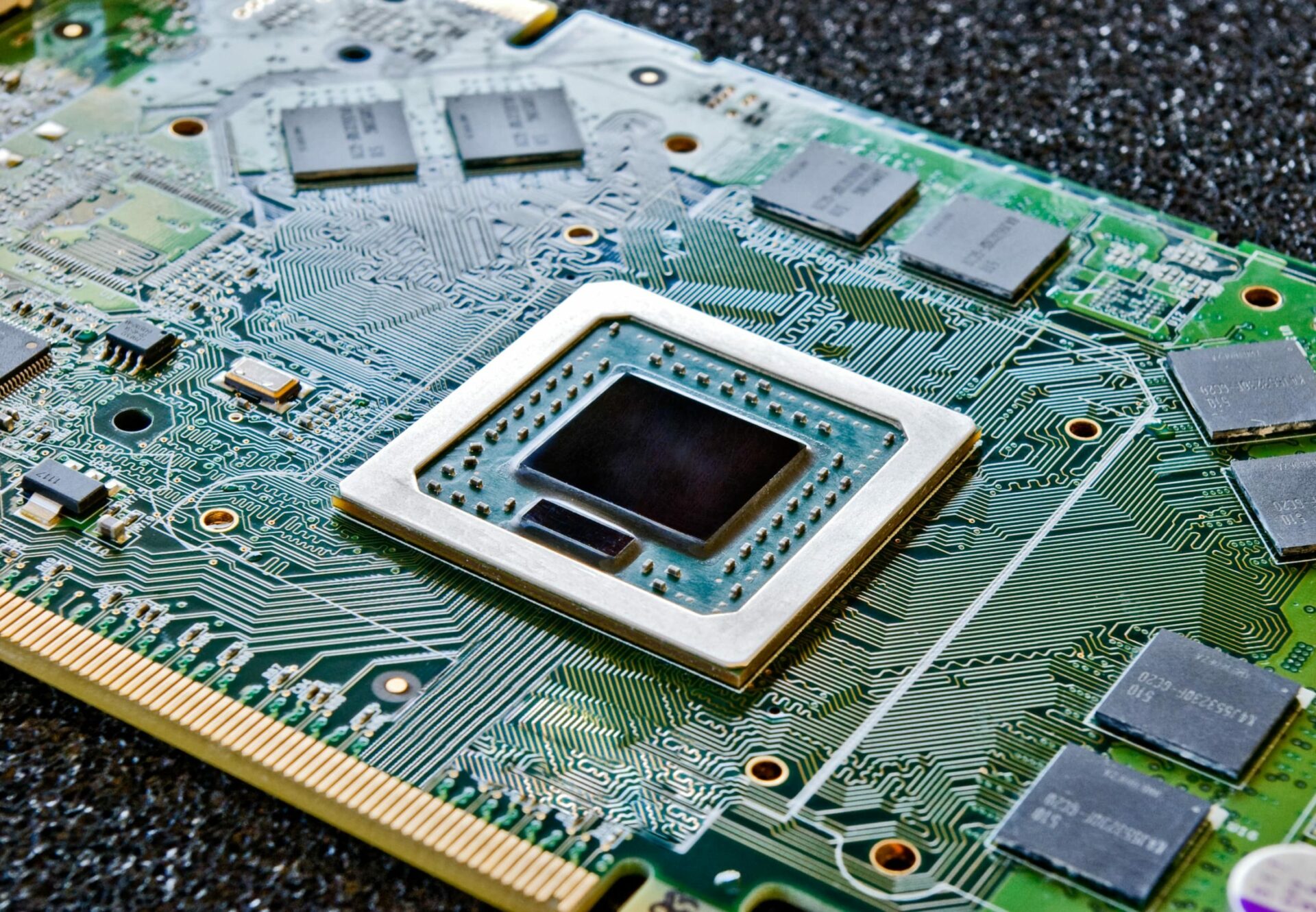
High density interconnect (HDI) printed circuit boards (PCBs) have emerged as an essential technology for many advanced electronics designs today. HDI PCBs allow routing of traces with extremely fine lines and spaces, enabling higher component densities and more compact layouts.
One of the key enablers of HDI PCBs are microvias – small vias with diameters typically under 150 microns. Microvias are critical for routing connections between the fine traces used in HDI designs. In addition to microvias, several other specialized via types have been developed for HDI PCBs.
This article provides an overview of the different via types used in HDI PCB routing and their characteristics.
Microvias
Microvias, as the name suggests, are vias with very small diameters, typically between 50-150 microns. The small size allows them to be placed between fine lines and spaces of traces in HDI designs. Microvias are essentially laser-drilled holes that connect between layers in an HDI stackup.
Some key properties of microvias:
- Diameter: 50-150 microns
- Capture pads: Same as trace width, unlike standard vias
- Pitch: 150-300 microns
- Aspect ratio: 1:1 to 4:1
- Plating: Electroless copper with electroplating
Microvias enable connections between the inner layers of an HDI stackup. This allows tracing routing capabilities that are not possible with standard through-hole vias. Microvias are the most common and important via type used in HDI PCBs.
Buried Vias
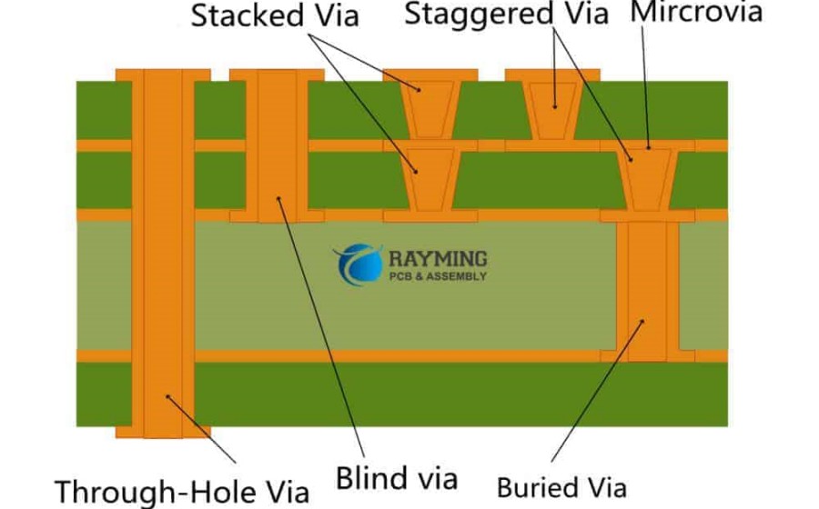
Buried vias are vias that connect between inner layers of a PCB without connecting to an outer layer. They are essentially “buried” within the PCB stackup.
Show Image<p style=”text-align:center”>*Image source: https://www.pcbcart.com/article/content/images/2021/06/Buried-Via-scaled.jpg*</p>
Some key properties of buried vias:
- Similar dimensions as microvias
- Connect only between inner layers
- Require planning in layer stackup design
- Allow greater routing flexibility
Buried vias avoid consuming routing space on outer layers, enabling higher routing density. They do require more complex stackup planning.
Blind Vias
Blind vias connect an outer layer of a PCB to one or more inner layers, without passing completely through the PCB.
Show Image<p style=”text-align:center”>*Image source: https://www.allaboutcircuits.com/uploads/thumbnails/via3_thumbnail.png*</p>
Key properties of blind vias:
- Connect outer layer to one or more inner layers
- Diameters from 150 microns to 300+ microns
- Require planned layer stackups
- Provide routing flexibility without consuming outer layer space
Blind vias avoid the need for through-hole vias when routing outer layers to inner layers. This helps maximize routing density.
Stacked Vias
Stacked vias consist of vias stacked vertically between PCB layers to form a conductive channel. The stacked vias can be microvias, buried vias, blind vias, or a combination.
Show Image<p style=”text-align:center”>*Image source: https://www.researchgate.net/profile/Yogendra-Mishra-2/publication/327379095/figure/fig3/AS:669299162681356@1536532174845/Schematic-of-stacked-via-structure-a-Across-section-view-b-3D-view.ppm*</p>
Key properties of stacked vias:
- Vertical stacking of multiple vias
- Allows routing connections between non-adjacent layers
- Optimizes layout by reducing surface routing
- Can be challenging to manufacture
Stacked vias minimize horizontal trace lengths by providing direct vertical connections between layers.
Skip Vias
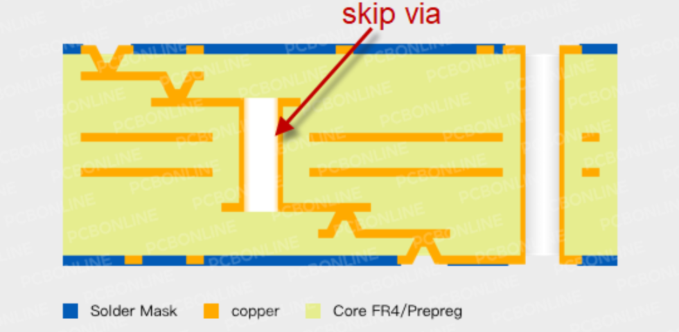
Skip vias are a type of stacked via where some layers are skipped in the vertical stack. For example, a skip via may connect Layer 1 to Layer 3, skipping over Layer 2.
Show Image<p style=”text-align:center”>*Image source: https://www.researchgate.net/profile/Yogendra-Mishra-2/publication/327379095/figure/fig4/AS:669298899521536@1536532175022/Schematic-of-skip-via-a-Across-section-view-b-3D-view.ppm*</p>
Key properties of skip vias:
- Vertical stack skipping over some layers
- Optimization of routing connections
- Avoid consuming routing resources on skipped layers
- Require planned layer stackups
Skip vias optimize vertical routing by skipping non-essential layers in the stacking.
Via-in-Pad
Via-in-pad (VIP) consists of vias placed within surface mount component pads. This allows connections from the component pads directly into inner layers.
Show Image<p style=”text-align:center”>*Image source: https://www.epectec.com/content/images/2021/09/Via-in-pad.jpg*</p>
Key properties of VIP:
- Vias placed within component footprint pads
- Allows direct connection from pads to inner layers
- Enables high-density routing under components
- Requires component pad size planning
VIP minimizes the need for surface traces between component pads and vias. This results in a more optimized, cleaner routing.
Summary Comparison
Here is a summary comparison of the key HDI via types:
| Via Type | Description | Key Properties |
|---|---|---|
| Microvia | Small vias, 50-150um diameter | Laser-drilled, fine pitch, 1:1 to 4:1 aspect ratio |
| Buried Via | Connect inner layers only | Avoid outer layer routing |
| Blind Via | Outer to inner layer | Avoid through-hole, optimize routing |
| Stacked Via | Vertical stacking of vias | Non-adjacent layer connections |
| Skip Via | Vertical stack skipping layers | Optimize vertical routing |
| Via-in-Pad | Vias in component pads | Direct pad to layer connections |
HDI Via Design and Manufacturing
There are some key considerations for designing and manufacturing the variety of vias used in HDI PCBs:
- HDI stackup planning – The layer stackup must be planned to support the various HDI via types such as blind, buried, and skip vias. This requires coordination between the designer and PCB manufacturer.
- Laser drilling – Microvias are typically laser drilled. Maintaining drill accuracy and quality at small diameters requires advanced laser drilling equipment.
- Via tenting – Blind and buried vias are often tented (covered) on layers they do not connect to. This requires tenting processes to avoid shorting.
- Plating challenges – Getting uniform plating coverage inside deep, small diameter microvias can be challenging. Additive plating processes are often used.
- Via reliability – HDI vias are prone to reliability risks such as cracking due to higher aspect ratios. Testing and standards compliance is critical.
- Manufacturing capability – HDI boards with dense microvias and other advanced via types require manufacturers with specialized equipment and processes.
HDI Via Design Guidelines
Here are some key guidelines for reliable HDI via design:
- Maintain at least 2:1 via diameter to hole spacing ratio
- Use capture pads equal to trace width for best registration
- Minimize unsupported via spans to reduce mechanical stress
- Limit via aspect ratios to 5:1 or less
- Plan layer transitions to enable blind/buried vias where possible
- Use stacked vias when connecting non-adjacent layers
- Incorporate via-in-pad to optimize routing under components
- Follow manufacturers design rules and stackup requirements
Following these guidelines will help produce a robust, manufacturable HDI board design.
Applications of HDI Vias
Some examples of products using HDI PCBs enabled by advanced via structures:
- Smartphones – HDI interconnects for high density components and flexible printed circuits
- Wearables – Using stacked microvias to connect double sided circuits
- Medical devices – Microvias for traces between implantable device layers
- Automotive – Low inductance microvias in power circuits for EVs and ADAS
- Aerospace – High reliability PCBs with microvias for avionics and guidance
- IoT devices – Compact PCBs with microvias for sensor connectivity
As electronics continue getting more compact and complex, HDI PCBs with advanced vias will become increasingly important across industries.
Conclusion
In summary, HDI PCB technology depends on the use of specialized via structures like microvias, buried vias, blind vias, and skip vias. These vias enable high density routing not possible with standard PCBs, while minimizing layout space and maximizing electrical performance. Correct design and fabrication is key to achieving reliable HDI boards. As electronics advance, HDI PCBs will continue to provide interconnect solutions for sophisticated and compact products across industries.
Frequently Asked Questions
Here are some common questions about HDI vias:
Q: What is the key benefit of microvias?
A: The small size of microvias, down to 50 microns diameter, allows them to be placed within the fine trace spacing in HDI designs. This enables routing density not achievable with standard vias.
Q: When would buried vias be used?
A: Buried vias connect between inner layers only. They help optimize routing by avoiding consumption of outer layer space that would be required for through-hole vias.
Q: What are some challenges with stacked vias?
A: Stacked vias can be difficult to reliably manufacture due to achieving uniform plating thickness down small, deep holes. The high aspect ratio also increases mechanical stress.
Q: How can skip vias optimize a design?
A: Skip vias provide direct vertical connections between non-adjacent layers, skipping over layers that don’t require connections. This minimizes the need for horizontal trace lengths.
Q: What is a key benefit of via-in-pad technology?
A: Via-in-pad places vias directly within component footprint pads, eliminating the need for traces between pads and vias. This allows very high density routing beneath components.


Leave a Reply