Introduction
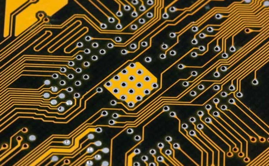
HDI (High Density Interconnect) PCBs are printed circuit boards with higher wiring densities than conventional PCBs. HDI technology allows traces and spaces between traces to be reduced to smaller dimensions, allowing more signal routing in the same area. This enables products to be made smaller and more compact with increased functionality.
HDI PCBs require special design considerations and manufacturing processes compared to standard PCBs. In this article, we’ll explore what makes HDI PCBs unique and discuss key differences in HDI design and manufacturing.
HDI PCB Design Differences
Designing an HDI PCB requires advanced skills and specialized software tools. Here are some of the key design differences compared to standard PCBs:
Smaller Traces and Spaces
The most obvious characteristic of HDI PCBs are the finer trace widths and smaller spacing between copper traces. While standard PCBs have minimum trace widths of around 6 mils, HDI PCBs can have trace widths down to 3 mils. And spacing between traces can be reduced to 3 mils as well.
| PCB Type | Minimum Trace Width | Minimum Trace Spacing |
|---|---|---|
| Standard PCB | 6 mils | 6 mils |
| HDI PCB | 3 mils | 3 mils |
More Routing Layers
To achieve the higher wiring densities, HDI PCBs utilize more copper routing layers. A typical HDI PCB may have 8-10 routing layers compared to only 4-6 layers on standard PCBs.
The additional layers allow traces to be “buried” inside the board where densities can be higher. Vias are used to connect traces between layers.
Smaller Vias
With the finer trace widths, the drill diameters for vias also need to be smaller on HDI PCBs. Microvias with diameters as low as 0.15mm are common. Laser drilling is used to create these microvias.
The small via sizes allow for a higher via density, permitting connections between layers without taking up as much space.
Tight Component Spacing
The components mounted on HDI PCBs will generally have tighter pitch spacing between leads or pads. Common component spacings are 0.4mm to 0.65mm.
To match this, the pad geometries on the PCB need to be proportionately smaller. High accuracy is required when designing pad shapes and spacings.
Tighter Tolerances
Overall, the design of HDI PCBs demands much tighter tolerances. Trace widths, spacings, drill diameters, and pad geometries require precision down to microns. This requires advanced PCB CAD tools and designer expertise.
HDI PCB Manufacturing Processes
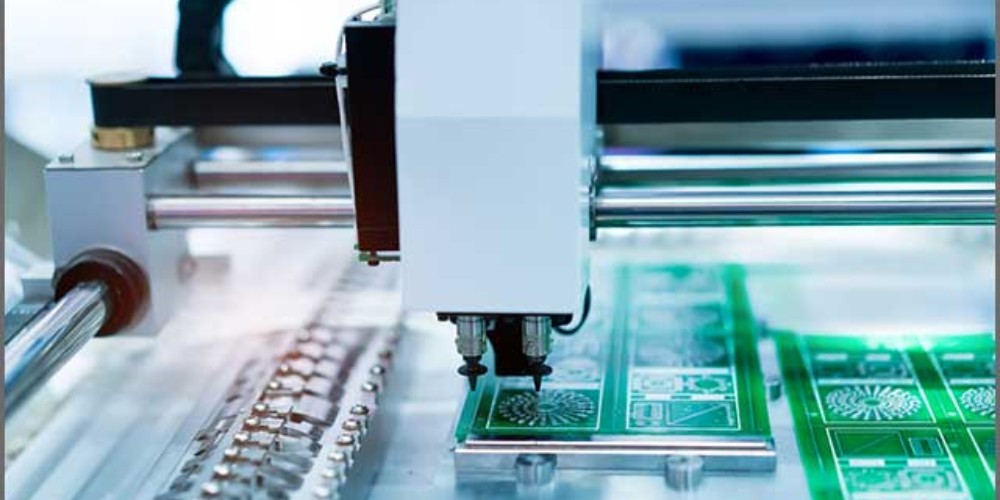
Fabricating HDI PCBs requires specialized manufacturing equipment and processes to produce the boards cost effectively in high volume. Here are some of the unique aspects of HDI PCB production:
Layer Lamination
The process of laminating together the layers of resin and copper foil is critical for HDI PCBs. The bonding between layers must be highly consistent across the board to avoid reliability issues from delamination or cracking under thermal stress.
To ensure accuracy, laser drilled microvias are often used to align layers and produce high layer-to-layer alignment precision.
The lamination process parameters including pressure, temperature, and curing time must be optimized to suit the board materials used.
Laser Drilling
As mentioned above, microvias on HDI PCBs are typically drilled with laser systems. Laser drilling can create small accurate holes down to 0.15mm diameter with good sidewall quality.
Careful process control is needed for laser drilling to produce consistent hole sizes across the board and between boards in a panel.
Plating Quality
To achieve reliable interconnects, the copper plating of traces and microvias must be very consistent and reliable. Plating processes like pattern plating and panel plating are used to ensure uniform plating thickness across the board.
Solder Mask Registration
Applying solder mask accurately is critical due to the tight tolerances. Solder mask registration precision down to ±0.025mm is common. Advanced optical inspection techniques are used to guarantee accuracy.
Via Protection
Microvias are susceptible to reliability issues like cracks or delamination around the thin copper barrels. Additional process steps may be used to reinforce microvias such as plugging, capping, or tenting.
Testing
100% electrical testing of HDI boards is strongly recommended to screen any potential defects. Automated Optical Inspection (AOI) and X-ray inspection can also help catch subtle flaws not detectable by testing alone.
Benefits of Using HDI PCBs
Here are some of the major benefits that can be achieved by utilizing HDI PCB technology:
- Higher component density allowing products to be made more compact and smaller
- Ability to route dense, complex interconnections
- Improved electrical performance from tightly controlled impedances
- Allows integrating more functionality in the same PCB area
- Reduces layer count for a given number of routing channels
- Facilitates miniaturization and portability of products
HDI PCB technology enables electronics manufacturers to design smaller, lighter, and more powerful devices to meet market demands. Products like smartphones, wearables, IoT devices, and advanced driver assistance systems for automotive rely on HDI PCBs. The technology will continue growing in usage as electronics and interconnected products continue getting more complex and compact.
Frequently Asked Questions About HDI PCBs

What are some typical applications for HDI PCBs?
Some of the most common applications for HDI PCBs are consumer electronics like smartphones, tablets, and wearables. They are also heavily used in communications infrastructure and telecom networking hardware. Other key uses are in aerospace, defense, automotive electronics, and medical devices. Basically any application where density, reliability and precision are important can benefit from HDI PCB technology.
How much more expensive are HDI PCBs compared to standard PCBs?
Due to the more complex manufacturing processes involved, HDI PCBs are generally 20% to 50% more expensive than equivalent standard PCBs for moderate production volumes. However, for very high volume consumer devices like smartphones, the costs can approach those of conventional PCBs.
Can components be mounted on both sides of HDI PCBs?
Yes, HDI PCBs can utilize SMT components on both sides of the board. Often, a mix of high density fine pitch components are used on the top side, along with larger pitch connectors or low density components on the bottom side. Careful layout is needed to route dense interconnects between top and bottom side components.
Are there limitations on board size for HDI PCBs?
There are not inherent size limitations, but typically HDI PCBs are smaller in size than standard PCBs. Common dimensions range from 20mm x 20mm up to about 300mm x 300mm. Very large boards are not well suited to the intricate manufacturing processes required. Stiffeners may be needed to prevent warpage on larger boards.
How many HDI layer types are there?
There are three main types of HDI layer stackups defined, although hybrid versions are also possible:
- Type I: One or more full uninterrupted plane layers.
- Type II: Stack of microvias connects two offset pad layers.
- Type III: Stack of microvias connecting traces on multiple layers.
The layer stackup configuration depends on routing requirements and can incorporate combinations of standard and HDI layer types.
Are special design skills required for HDI PCBs?
Yes, to fully leverage the benefits of HDI technology and avoid potential pitfalls, PCB designers should have specialized training and experience. HDI design requires expertise with advanced PCB CAD tools as well as an understanding of HDI manufacturing processes and capabilities to avoid design for manufacturability issues. Most PCB designers need to accumulate years of experience before tackling complex HDI designs.
How are impedances controlled on HDI PCBs?
Maintaining tight impedance tolerances is critical for signal integrity, especially for high speed designs. Some methods for impedance control include:
- Selecting PCB materials with consistent dielectric properties
- Maintaining careful thickness uniformity across layers
- Using plane layers for impedance reference
- Matching trace widths to required impedance
- Choosing laminate materials with low dielectric loss
Simulation and modeling tools are used to design controlled impedance interconnects and verify impedance targets will be met.
Conclusion
HDI PCB technology enables dense routing and integration of complex electronics in smaller packages. This is driven by market demands for ever more compact and capable wireless devices and products.
While sharing some commonalities with conventional PCBs, HDI introduces finer geometries, tighter tolerances, and advanced manufacturing processes. Careful HDI-specific design practices and close collaboration with the PCB manufacturer are key to producing functional, reliable HDI boards cost effectively.
As electronics continue getting more sophisticated and incorporated into more aspects of our lives, HDI PCBs will be essential for integration and keeping products as small and portable as possible.


Leave a Reply