Introduction
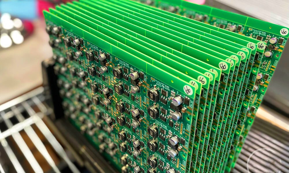
High density interconnect (HDI) printed circuit boards (PCBs) have become increasingly popular in recent years due to the growing demand for smaller and more complex electronic devices. As components shrink in size and increase in number, PCB designers must find ways to accommodate all the necessary interconnects in a limited space. This has led to continual innovations in HDI technology to achieve greater interconnect density and routing complexity.
One of the most advanced HDI technologies today is known as Every Layer Interconnection (ELIC). ELIC represents the ultimate evolution of HDI, allowing connections between any and all layers of a multilayer PCB stackup. This enables routing traces and vias between any two layers, not just adjacent ones. As a result, ELIC provides the highest possible interconnect density and design flexibility for complex, high-speed PCBs.
What is ELIC?
ELIC technology utilizes a combination of laser drilling, plasma etching, and advanced buildup materials to fabricate a PCB with interconnects passing through and between any layers. This is accomplished through three key innovations:
1. Sequential Buildup Layers
Rather than laminating all layers together at once, ELIC uses a sequential process to build up the PCB layer by layer. This allows the drilling and metallization of microvias as each layer is added.
2. Microvias
Tiny vias with diameters below 0.15 mm are drilled using advanced laser systems. Microvias enable connections between any layers in the stackup.
3. Filled Vias
Instead of leaving vias hollow, ELIC fills them with a plasma-etched metallization. This allows traces to be routed across the filled vias on adjacent layers.
By integrating these three features, ELIC boards can have signal routing and component connections between any layers. This enables true any-to-any layer interconnects within a PCB.
Advantages of ELIC HDI
The ELIC approach provides a number of important benefits for advanced HDI PCBs:
- Increased Routing Density – With any-angle routing between layers, ELIC allows up to 4x greater interconnect density compared to traditional HDI.
- Design Flexibility – ELIC enables connections between non-adjacent layers, removing routing constraints and gaps.
- Complex Layouts – Unrestricted layer-to-layer routing facilitates highly complex layouts for advanced components.
- Signal Integrity – Direct layer-to-layer paths improve signal speeds, timing, and signal integrity.
- Miniaturization – ELIC allows more functionality to fit into a given PCB footprint area.
- Thin Stackups – By eliminating constraints, ELIC enables thinner overall board stackups.
In essence, ELIC represents the state-of-the-art for maximizing interconnect density, routing flexibility, and miniaturization in advanced PCBs.
ELIC Design and Fabrication
Implementing ELIC technology requires specialized design and manufacturing processes:
ELIC Design
ELIC layouts leverage advanced PCB CAD tools for:
- Planning layer stackups
- Assigning nets to any layer
- High-speed signal integrity analysis
- 3D modeling of complex space constraints
- Generating bill of materials, fabrication, and assembly data
The increased complexity demands coordination between layout designers and electrical engineers.
ELIC Fabrication
The ELIC sequential buildup process allows production of multilayer boards with up to 30 or more layers. Each core and buildup layer is processed individually:
- Metallization – Sputtered copper is electroplated to desired thickness on each layer.
- Microvia Drilling – Microvias are lasered between layers requiring interconnects.
- Via Filling – Copper electroplating fills the vias flush to the layer surface.
- Imaging – Layers are coated with photoresist and imaged to define trace patterns.
- Etching – Exposed copper is etched away, leaving traces and bond pads.
- Layer Bonding – Adhesive films bond the layers into a complete stackup.
- Outer Layers – Final imaging and etching defines the outer layer traces and features.
The critical steps of laser drilling and plasma via filling must achieve high accuracy and reliability.
Applications of ELIC
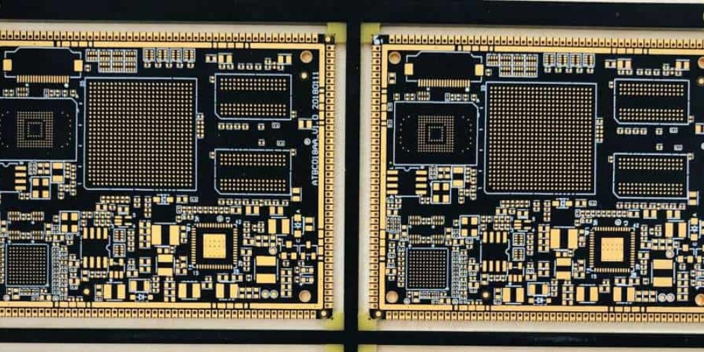
The unmatched interconnect density of ELIC makes it an enabling technology for leading-edge electronic systems, including:
High-Speed Digital Electronics
- Advanced server, network switch, and router PCBs
- Next-generation telecom/datacom equipment
- High-performance computing systems
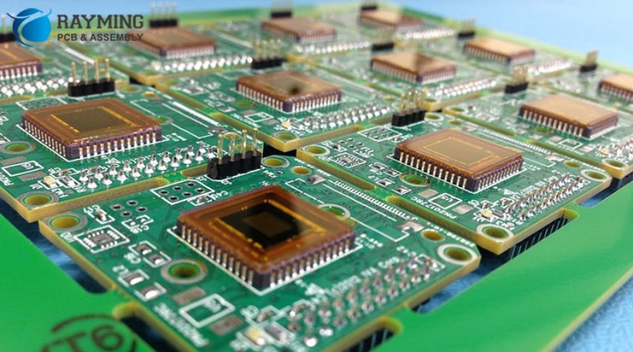
Advanced IC Packaging
- Interposers for 2.5D and 3D chip stacking
- Fine-pitch flip chip package substrates
- High I/O density BGA/CSP packages
Military/Aerospace
- Radar and electronic warfare systems
- Satellite payloads
- Missile guidance systems
Medical Electronics
- Implantable devices
- Hearing aids
- Diagnostic imaging equipment
ELIC provides the interconnect capability to support integrating cutting-edge ICs into innovative, miniaturized products for these demanding applications.
The Future of ELIC
As electronic devices continue advancing towards higher speeds, greater functionality, and smaller sizes, PCBs will require increasing interconnect densities. This will drive ELIC to become more widely adopted in the industry.
However, realizing the full benefits of ELIC technology will depend on continued progress in key areas:
- Improving design tools – More automation and analysis features will be needed to fully leverage ELIC’s routing flexibility.
- Scaling microvia dimensions – Smaller microvias will enable greater interconnect density as fabrication processes improve.
- Increasing reliability – Maintaining robust connections will require advances in microvia drilling, filling, and layer bonding.
- Lowering costs – Developing volume production methods can make ELIC more affordable for the commercial electronics market.
With ongoing innovation, Every Layer Interconnection will become the new standard, enabling another generation of electronics advancement.
Frequently Asked Questions

What are the key technologies that enable ELIC HDI boards?
The three critical innovations that allow any-to-any layer interconnects in ELIC boards are:
- Sequential buildup of individual layers
- Ultra-high density microvias lasered between layers
- Filled microvias using plasma-etched metallization
Together these manufacturing advances provide connections between any layers within the multilayer stackup.
How small can microvias be with current ELIC technology?
Using advanced laser drilling techniques, ELIC microvias can achieve diameters between 50-150 μm (0.050-0.150 mm). This allows over 100,000 interconnects per square inch between layers. Microvia scaling below 50 μm is a major focus for further improving ELIC interconnect density.
What are the main application areas currently using ELIC technology?
The leading users of ELIC HDI today are in high-speed digital electronics, IC packaging, military/aerospace, and advanced medical devices. These applications require the highest interconnect densities to accommodate their complex electronic designs. ELIC provides the routing flexibility needed in the smallest form factors.
Does ELIC require any special PCB design practices?
Yes, to fully utilize ELIC’s any-to-any layer routing capability, designs must employ advanced modeling, analysis, and layout techniques. This includes 3D modeling of the layer stackup, signal integrity analysis, thermal analysis, and design rule checks tailored to ELIC buildup processes. The design complexity also demands close teamwork between schematic, layout, and fabrication engineers.
How does ELIC compare to other HDI technologies?
ELIC represents the leading edge of HDI technology today, enabling the highest interconnect density and greatest routing flexibility. It provides 4x the routing density of standard HDI, 2x that of advanced sequentially laminated HDI, and 1.5x that of skip-via HDI. However, ELIC also requires specialized design and fabrication processes that can increase costs compared to other HDI approaches.
Conclusion
ELIC HDI delivers unmatched interconnect density and routing flexibility for advanced PCBs. By allowing any-to-any layer routing using microvias, ELIC can accommodate extremely complex component layouts and circuit connectivity. This enables innovative electronics designs in high-speed digital, IC packaging, military/aerospace, and medical product applications. While specialized fabrication methods are needed, ongoing improvements will spread adoption to meet demands for ever-greater functionality and miniaturization. ELIC paves the way for the next generation of electronics innovation.


Leave a Reply