
Introduction
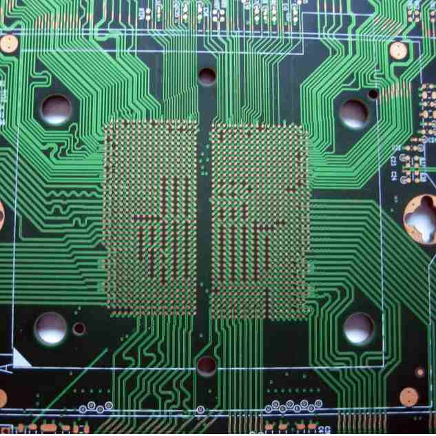
High-density interconnect (HDI) PCBs have become increasingly popular in recent years due to the continued miniaturization of electronics. HDI allows for tighter routing spaces, more signal layers, finer lines and spaces, microvias, and other features not possible on conventional PCBs.
The 1+N+1 HDI stackup is one of the simplest HDI configurations, making it an ideal choice for many designs that need higher density without the complexity of a full build-up process. In this article, we will explore what 1+N+1 HDI is, its benefits, design considerations, and assembly challenges.
What is 1+N+1 HDI?
1+N+1 refers to the layer stackup construction:
- 1: Top microvia layer
- N: Number of sequential laminated inner layers
- 1: Bottom microvia layer
For example, a 1+4+1 HDI PCB would have:
- 1 layer on top with microvias
- 4 sequential laminated inner layers
- 1 layer on bottom with microvias
The top and bottom outer layers allow for microvias, while the inner N layers are conventional laminated layers without microvias.
Benefits of 1+N+1 HDI
Compared to conventional PCB layer stackups, 1+N+1 HDI offers several advantages:
- Higher routing density: Microvias allow connections between layers with a smaller drill size and capture pad than through-hole vias, enabling tighter trace spacing.
- More layer counts: By adding thin dielectric build-up layers on the outer surfaces, you can increase the total layer count beyond the limits of sequential lamination.
- Fine lines and spaces: Line width/spacing down to 2/2 mil (0.05mm) is possible with 1+N+1 HDI depending on board shop capabilities.
- Lower costs: 1+N+1 HDI avoids the complexity and expense of a full dense interconnect structure. It’s an affordable step into HDI for many designs.
In summary, 1+N+1 allows you to achieve some of the key benefits of HDI while minimizing fabrication process changes from conventional PCBs. It’s a scalable, cost-effective HDI solution.
1+N+1 Design Considerations
While simpler than full build-up HDI, designing 1+N+1 boards still requires some special considerations:
Routing:
- Stacking microvias can connect between any layers. This enables creative routing solutions but can also create confusion. Using a grid system for traces and vias can help organize routing.
- Lightly loaded layers may cause acid traps during processing. Filling space with dummy features helps balance surface area.
- Minimize unsupported microvia spans to control film cracking. Unsupported spans longer than 15 mils increase risk.
Materials:
- Dielectric build-up materials are typically 25-50um thick for each layer, with εr of 3.5-3.9. This affects impedance calculations.
- Metal cores may be used for very thin dielectrics. Prepregs bond poorly to some metal core types.
- Resins used for build-up materials have different CTEs than the laminated dielectric. This can impact reliability.
Stackup:
- A thicker cut layer, like 0.012” (0.3mm), is preferred closest to the build-up layers to provide mechanical support.
- Avoid placing heavily routed layers adjacent to build-up layers as this makes alignment challenging.
- Ensure microvia capture pads don’t encroach on sequential laminated layers. Allow for registration tolerances.
HDI PCB Assembly Challenges
While 1+N+1 HDI provides many benefits, it also creates some challenges for PCB assembly:
- Via in pad (VIP): Microvias in surface mount lands prevent solder wicking into the hole. This can lead to incomplete pad fills. Filling vias or reducing via size helps.
- Microvias underneath BGAs: Unfilled vias under BGA packages alter solder ball collapse. Mitigation strategies like via filling or dummy vias are needed.
- Thinner cores: Thin dielectrics are prone to warping which complicates assembly. Rigid-flex techniques may be required.
- Pad tolerance: Tighter laser-drilled microvias call for tighter pad tolerances. This demands improvements in fabrication capability and soldermask registration.
- New materials: Coefficients of thermal expansion (CTEs) can vary between build-up dielectrics and laminates. Thermal cycling reliability may require evaluation.
While these factors raise the complexity of assembly, they are manageable with thoughtful design and controlled process development.
Example of 1+N+1 Stackup Construction
To illustrate a 1+N+1 stackup, let’s look at a specific 6 layer design:
| Layer # | Layer Type | Thickness |
|---|---|---|
| 1 | Top Microvia | 25um dielectric / 18um copper |
| 2 | Signal | 0.5 oz copper / 7628 prepreg |
| 3 | Ground | 1 oz copper / 7628 prepreg |
| 4 | Signal | 0.5 oz copper / 7628 prepreg |
| 5 | Bottom Microvia | 25um dielectric / 18um copper |
| 6 | Signal | 0.5 oz copper |
This breakdown shows:
- 2 signal layers in 0.5 oz copper with conventional 7628 prepreg dielectric
- 1 ground layer in 1 oz copper for noise isolation
- 25um dielectric build-up layers on top and bottom with 18um copper traces
The thin build-up dielectrics allow microvias, enabling a 6 layer board with high density interconnects. Components can connect between the top and bottom microvia layers or interface anywhere within the stackup.
Summary
The 1+N+1 HDI configuration provides an affordable stepping stone into the benefits of high density PCBs. By adding thin microvia dielectric layers to a conventional laminated core, routing density increases without the complexity of full build-up constructions. This enables finer lines and spaces, higher layer counts, better noise isolation, and more flexibility for advanced IC packaging.
However, the approach also introduces new considerations around materials, stackup, and assembly. An HDI-capable PCB fabricator is key, as 1+N+1 demands tighter tolerances. When designed thoughtfully, 1+N+1 HDI can elevate a PCB’s performance without breaking the budget. For products pushing the edge of miniature electronics, it’s an enabling technology that packs a lot of capability into a small space.
Frequently Asked Questions
What are some typical applications for 1+N+1 HDI PCBs?
Some common applications that benefit from 1+N+1 HDI include:
- Smartphones, tablets, and other mobile devices where space is extremely limited. The high routing density allows more functionality.
- Advanced IC packaging like SiP and SoC designs that integrate multiple dies. HDI provides the interconnect density for chip-to-chip communication.
- High speed digital design with many channels. The additional layers provide routing channels and microvia shielding.
- RF circuits operating above 5GHz. Tight conductor spacing and via placement are necessary at high frequencies.
Is 1+N+1 HDI suitable for mixed signal or high speed analog?
It can be, but the utmost care must be taken in layout. Analog signals are very sensitive to cross-talk and stub effects. Provide adequate guard traces or ground shields around analog signals. Use stacking microvias to cross split ground planes. Minimize stubs by avoiding 90 degree routing corners. Simulations early in the design flow are recommended.
What panel and hole size limitations exist for 1+N+1 HDI PCBs?
Common panel sizes for 1+N+1 fabrication fall in the 18″x24″ (457mm x 610mm) range. Maximum hole size is typically 8mil finished diameter, allowing 6mil microvias on ±2 mil tolerance. Linear routing density of up to 800inches/inch2 is possible depending on line width/space.
Should I use PTHs or all microvias in a 1+N+1 design?
It’s generally better to use microvias where possible and limit PTHs. Microvias occupy less space on routing layers. Placing PTHs adjacent to microvia interconnects also creates challenges around capture pad tolerances. Use PTHs only where needed for mass interconnects, connectors, or components that cannot accommodate microvias.
What are recommended minimum trace widths and spaces for 1+N+1 HDI?
3/3mil line/space width is readily achievable. 2/2mil requires specialized processes with very tight registration capabilities. 1/1mil lines/spaces are possible but pushing the limits of fabricator tolerances. Keep high density routing on outer microvia layers and use inner layers for wider features.


Leave a Reply