Introduction
Printed circuit boards (PCBs) are essential components in almost all modern electronic devices. They provide the foundation on which chips, resistors, capacitors and other components are mounted and interconnected. For any new electronic product development, having custom PCBs manufactured is an important step.
A key consideration when getting PCBs made is the lead time – how long does the entire process take from initial design to received boards? The PCB manufacturing timeline can range from a few days to several weeks depending on the board complexity, order quantity and fabrication options. This article provides a detailed look at the typical PCB production stages and timescales.
PCB Design and Layout
The first step in the PCB production workflow is creating the board layout. This includes:
- Schematic capture – Drawing the electronic circuit schematics using CAD software. This translates the logical connectivity between components into a wiring diagram.
- PCB layout – Converting the schematic into the physical board layout. This involves arranging components and routing copper traces to connect them on a 2D plane.
- Design rule checks – Software tools verify the layout adheres to fabrication capabilities – things like track widths, clearance between copper, drill sizes etc.
For a simple PCB with just a few components, the design can be completed in a day or two. Complex boards with high component densities or challenging layout requirements can take weeks to finalize.
Generating Fabrication Files

Once the PCB layout is finalized, a set of fabrication files need to be exported:
- Gerbers – Standard files containing 2D vector artwork for each copper layer, solder mask, silkscreen etc.
- Drill file – NC drill file with tool locations and sizes to create holes.
- BOM – Bill of materials listing all components.
- Assembly drawings – Files to aid PCB assembly.
This process is automated using CAD software and can be completed in an hour or two.
Selecting a PCB Manufacturer
There are many PCB manufacturers to choose from. Key factors are:
- Capabilities – Available PCB technologies, minimum clearances etc. Important for high density or advanced boards.
- Lead times – How long to fabricate the boards. Typically 5-15 days.
- Quality – Consistency, reliability and attention to detail. Vital for volume production.
- Cost – PCB prices vary significantly. Need to balance with budget.
- Location – Local providers minimize shipping time and costs. Helpful for quick-turn requirements.
Choosing the right supplier involves researching companies and getting quotes. Allow 2-3 days for this process.
Placing a PCB Order
Once the manufacturer is selected, an order is placed by uploading the Gerber files and other data. Additional information is required:
- Quantities – Number of boards needed. Often start with small prototyping run.
- Lead time – Standard or expedited options. Faster times increase costs.
- Specifications – Board materials, finishes, thickness etc. Determines capabilities and price.
- Testing – Any fabrication testing like automated optical inspection.
- Shipping – Courier options.
Placing the order can be done in a few hours. The PCB company will review the order and provide a confirmed fabrication timeline.
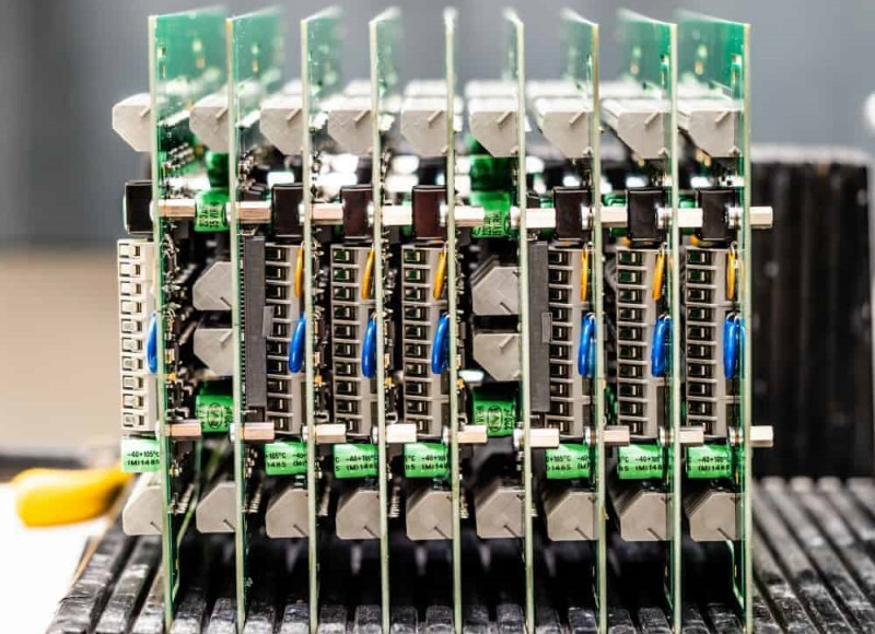
PCB Fabrication Process
The actual PCB production happens in a multi-stage process:
Layer Stack Patterning
The inner and outer layers are prepared first:
- Imaging – Photoresist is applied on copper clad laminate and imaged using lithography techniques. This forms a mask in the shape of the desired traces.
- Developing – Exposed areas of copper are etched away, leaving only the protected pattern.
- Stripping – Photoresist is removed, leaving finished copper layer artwork.
This creates the conductors on each layer that will be interconnected.
Layer Alignment and Bonding
Individual layers are precisely aligned and laminated together:
- Alignment – Using registration holes, artwork layers are stacked to ensure accurate trace positioning.
- Lamination – Layers are bonded using high temperature and pressure. This creates a complete board sandwich.
- Drilling – Holes are drilled for component leads and vias. Desmear removes resin smear.
Aligning layers accurately is critical for reliable interconnection.
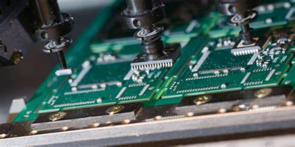
Final PCB Finishing
Final operations ready the boards for assembly and use:
- Conductive plating – Electroless plating makes drilled holes and vias conductive.
- Solder mask – Epoxy layer coated over copper to prevent solder bridging. Openings left for pads.
- Silkscreen – Printed markings identify components, polarity etc.
- Edge plating – Gold or tin-lead plating prevents edge copper oxidation.
- Testing – Electrical tests validate conductivity. Automated optical inspection checks fabrication accuracy.
These finishing steps protect the PCBs and complete manufacturing.
Lead Time Estimates
The full end-to-end timeline to get PCBs made depends on the key stages:
| Stage | Timeframe |
|---|---|
| PCB Design | 1-5 days (simple), 5-10 days (complex) |
| File Preparation | 1-2 days |
| Manufacturer Selection | 2-3 days |
| Order Placement and Review | 1 day |
| Fabrication | 5-15 days (standard), 2-5 days (expedited) |
| Shipping | 1-5 days |
Total typical lead time: 2-4 weeks
Here are some notes on the timeline:
- The design stage has the most variability based on complexity. It governs the overall schedule.
- Fast shipping or local manufacturers reduce transit time.
- Expedited fabrication reduces production time but increases costs significantly.
- Building margin into the schedule is recommended.
For low volume prototyping, target 3-4 week total lead time from design to delivery as a best practice. Adjust expectations for volume production or high complexity boards. Discussing timelines with the PCB manufacturer is always advised.
Factors That Impact Lead Time
Many factors can influence the PCB fabrication lead time:
- Order quantity – Small and mid-size orders typically ship faster than high volumes.
- Board size – Larger PCBs take longer in lamination and imaging processes.
- Layer count – More layers add alignment and lamination steps.
- Materials – Standard FR-4 is faster than high-Tg, ceramic or flex PCBs.
- Finishes – Immersion silver is quicker than ENIG or hard gold plating.
- Technology – HDI boards take longer than conventional fabrication.
- Tooling – New custom tools like press plates slow initial orders.
- Testing – In-circuit test, flying probe etc. increase lead time.
- Priority – Production scheduling affects lead time. Prototypes are usually expedited.
- Location – Local suppliers have shorter logistics time.
Evaluating the above factors relative to the PCB requirements helps estimate realistic timelines. Discussing with the manufacturer is the best way to confirm.
Strategies for Faster PCB Delivery
For projects with tight deadlines, here are some tips to help accelerate PCB fabrication and delivery:
- Select manufacturer carefully – Choose companies with reputation for on-time delivery and fast turns.
- Pay extra for expedited service – Almost all PCB companies offer quicker fabrication for a premium cost.
- Eliminate unnecessary complexity – Simplify the design wherever possible – fewer layers, standard materials etc.
- Submit order early – Provide fabrication files as soon as they are ready to get in production queue.
- Follow up frequently – Check order status and see if prioritization is possible. Make any file corrections quickly.
- Pay for faster shipping – Use express courier service to reduce transport time.
- Shift inventory ahead – Stockpile critical components early so PCBs can be immediately assembled on arrival.
While the PCB fabrication process has inherent time requirements, smart planning with the steps above can help reduce lead times.
Frequently Asked Questions
What is the quickest turnaround time for getting PCBs?
For simple boards, some manufacturers advertise 24-48 hour turnaround from order to delivery. More realistically, 5-7 days total can be achieved from design completion to receipt with an expedited order of basic 2-4 layer boards.
How can I get free PCB prototypes?
Many PCB companies offer discounted or free prototypes for new customers designing their first boards. Only a few boards are provided, but it allows evaluating quality and service.
Can I get same day PCB manufacturing?
While not typical, some manufacturers offer same day fabrication in select locations for an additional premium charge. The order must be placed early, boards cannot be complex, and local courier pickup is required.
What is the best PCB company for fast delivery?
There are a number of reputable PCB firms that provide quick turns including Advanced Circuits, PCBWay, Epic PCB and others. Comparing quotes and production times is recommended.
How much does expedited PCB fabrication cost?
Expediting services vary, but generally adding 3-5 days faster delivery increases cost by 25-50%. The minimum charge is usually $250-500. Very urgent 1-2 day turns can cost 2-3X standard pricing.
Conclusion
The full process to have PCBs made and delivered typically spans 2-4 weeks. The most variable factors are the design timeline and standard fabrication lead time. Expediting services and local suppliers can help shrink the schedule where needed, but often at a significant premium. Planning appropriately and working closely with the PCB manufacturer is key to setting realistic expectations on delivery.


Leave a Reply