Introduction
PCB stands for printed circuit board. A printed circuit board, or PCB, is a thin board made of fiberglass or other composite material used to mechanically support and electrically connect electronic components using conductive pathways or traces. PCBs provide the foundation for almost all modern electronics, from simple devices like calculators to complex computer systems and telecommunications equipment. Understanding what PCBs are and how they work is key to designing, building, and troubleshooting electronic circuits and devices.
What is a Printed Circuit Board?
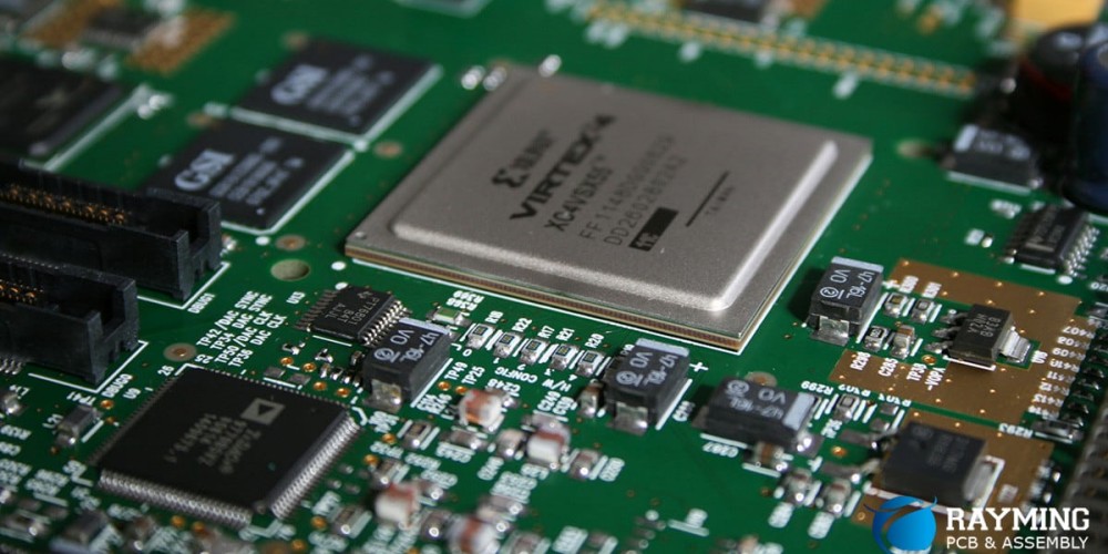
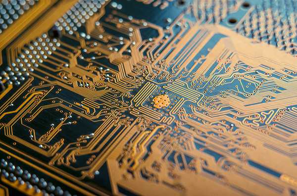
A printed circuit board (PCB) is a board made of insulating material, usually fiberglass, with thin copper foil bonded to one or both sides. The copper layer is etched into individual copper traces that interconnect various components mounted on the board. PCBs provide mechanical support and electrical connections between components in an electronic device.
Key Features of PCBs
- Insulating Substrate – Usually FR-4 fiberglass but can be other materials like ceramics or polyimides. Provides mechanical support.
- Copper Traces – The etched copper layer forms the conductive pathways between components.
- Solder Mask – Covers the copper traces for protection, except for exposed pads.
- Silkscreen – Used to print component outlines, labels, logos, etc. for identification.
- Plated Through-Holes – Holes drilled in the PCB with copper plating to allow connections between layers.
PCB Materials
The most common materials used in PCB fabrication:
- Substrate – FR-4 Glass Epoxy. Alternatives are ceramics and polyimides.
- Conductor – Copper foil. Sometimes nickel/gold plating is applied.
- Solder Mask – Liquid PhotoImageable Solder Mask (LPI).
- Silkscreen – Epoxy ink.
PCB Layout and Design
The PCB layout connects components with copper traces according to the circuit schematic requirements. PCB layout involves placement of components and routing of copper traces between their pads.
Steps in PCB Layout
- Place components based on connections
- Route traces point-to-point between pads
- Ensure design rules like trace width and spacing are followed
- Add text labels, logos, fills as needed
- Check clearances, test points, other criteria
- Verify electrical connectivity of completed layout
Key PCB Layout Factors
Some key factors to consider in PCB layout:
- Component placement for shortest traces
- Critical signal routing for controlled impedance
- Power plane for noise reduction and thermal relief
- High-speed design constraints
- EMI control with ground planes, shielding
- Thermal considerations like heat sinks
- Test points for troubleshooting
- Manufacturability and cost reduction
PCB Fabrication Process
Printed circuit boards go through many stages of fabrication to create the finished board. The main steps are imaging, etching, bonding, drilling, plating, and finishing.
PCB Fabrication Steps
- Imaging – Photoresist coated on copper is exposed to UV through the layout pattern film.
- Etching – Unexposed photoresist is developed away, exposing copper for chemical etching.
- Bonding – Layers are bonded together with epoxy resin prepreg.
- Drilling – Holes are drilled for component leads and vias.
- Plating – Copper is electroplated on hole walls for conductivity.
- Solder mask – Covers copper with epoxy except pads.
- Silkscreen – Prints reference designators, labels, logos.
- Finished board – Electrical testing performed before shipping.
Here is a summary table of the PCB fabrication process:
| Stage | Description |
|---|---|
| Imaging | Photoresist coated on copper is exposed to UV light |
| Etching | Exposed copper is etched away to form traces |
| Bonding | Layers are laminated together with prepreg |
| Drilling | Holes are drilled for vias and component leads |
| Plating | Copper is plated on drilled hole walls |
| Solder mask | Epoxy coating covers copper except solder pads |
| Silkscreen | Prints reference designators and identifiers |
| Finishing | Electrical testing before boards are shipped |
PCB Assembly
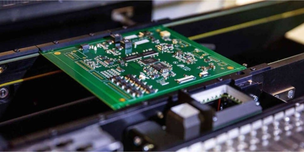
After fabrication, PCBs undergo assembly and soldering of components to produce a functional printed circuit board assembly (PCBA).
PCB Assembly Steps
The major steps in assembling component boards:
- Paste application – Solder paste is printed on pads for surface mount device soldering.
- Component placement – Robots and/or operators place components on pads.
- Reflow soldering – Solder paste is melted to attach SMDs during controlled heating.
- Through-hole insertion – Leaded components are inserted into plated through-holes.
- Wave soldering – Bottom side soldering of leaded components.
- Inspection and test – Ensures quality solder joints and reliable functionality.
- Conformal coating – Optional protective coating against environmental damage.
A summary of the assembly process:
| Stage | Description |
|---|---|
| Paste printing | Solder paste deposited on SMD pads |
| Component placement | SMDs placed on paste sites |
| Reflow soldering | Heat melts solder to attach components |
| Through-hole insertion | Leaded components inserted |
| Wave soldering | Solder bottom side leaded joints |
| Testing and inspection | Validates assembly and soldering quality |
| Conformal coating | Optional protective coating |
PCB Classifications
There are several classifications of PCBs based on the number of layers or based on functionality:
Number of Layers
- Single-sided – Copper traces on one side only.
- Double-sided – Copper on both sides of the substrate.
- Multilayer – More than 2 copper layers, allows greater complexity.
Functionality
- Analog PCBs – Designed for analog circuits like amplifiers. Use large ground planes to reduce noise.
- Digital PCBs – Optimized for fast digital signals. Controlled impedance traces, isolation between channels.
- RF/Microwave PCBs – High frequency performance, controlled impedances. May use exotic materials.
- Flex/Rigid-Flex – Flexible boards that can bend and fold. Used where flexibility is required.
Here is a summary table of some common PCB classifications:
| Classification | Description |
|---|---|
| Single-sided | Copper traces on one side |
| Double-sided | Copper on both sides |
| Multilayer | More than 2 copper layers |
| Analog | Designed for analog circuits |
| Digital | Optimized for fast digital signals |
| RF/Microwave | High frequency performance |
| Flex/Rigid-Flex | Flexible bending boards |
PCB Design Software
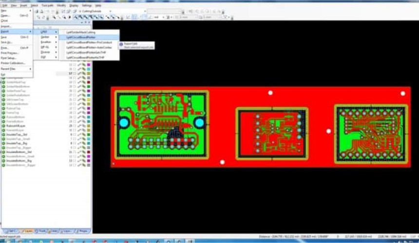
To help automate and streamline PCB design, engineers use electronic design automation (EDA) software. Popular options include:
- Altium Designer – High-end PCB design platform with unified environment.
- Eagle – Affordable PCB design with schematic capture and board layout. Now owned by Autodesk.
- KiCad – Open source PCB design software with full feature set.
- OrCAD – Part of Cadence design suite, integrates with Allegro PCB Editor.
- PADS – Feature-rich PCB design from Mentor Graphics, part of Siemens EDA.
- Zuken CR-8000 – High-speed design, signal and power integrity analysis.
The main stages supported by PCB design EDA tools:
- Schematic capture – Create circuit schematics
- Board layout – Layout components and route copper traces
- Design rule checks – Verify manufacturability
- Simulation – Simulate circuit behavior
- Manufacturing output – Generate files for fabrication
Applications of PCBs
Printed circuit boards are found in almost every modern electronic device. Some examples applications and products:
- Computers – Motherboards, graphics cards, storage devices
- Consumer electronics – Phones, TVs, gaming systems
- Automotive – Engine control units, infotainment, sensors
- Aerospace and defense – Avionics, radar, guidance systems
- Medical – Diagnostic systems, surgical tools, implants
- Communications – Routers, base stations, switches
- Industrial – Programmable controllers, robotics, CNC machines
Virtually every electronic product relies on PCBs to provide the underlying interconnect foundation. They enable communication between ICs and discrete components, bringing electronic system designs to life.
PCB Trends and Innovations
Some current trends and innovations in PCB technology and fabrication include:
- Miniaturization – Shrinking component sizes drive demand for tighter trace pitches.
- High density interconnects (HDI) – More routing layers allow complex functionality in small form factors.
- Embedded passives – Capacitors and resistors embedded directly into the PCB itself.
- Flex and rigid-flex – Boards can flex and bend dynamically.
- Additive manufacturing – Printed circuit traces using 3D printing-like techniques.
- 5G networks – High speed design for mmWave frequencies.
- Automation – More automation of assembly and optimized production.
Continued innovation in materials, design, and manufacturing allows PCBs to advance in terms of capability, performance, and cost-effectiveness.
Conclusion
In summary, the printed circuit board provides the foundation for electronic devices and products by interconnecting components using conductive copper traces etched from copper foil. PCBs go through complex fabrication processes to create multilayer boards that allow complex circuit designs. Continual innovations in PCB technology allow electronic devices and systems to become ever more advanced and compact. Understanding what PCBs are and how they are designed and manufactured is key for anyone involved in electronics and circuit design.
Frequently Asked Questions
What are the main components of a PCB?
The main components of a typical PCB are the insulating substrate material, the conductive copper traces, solder mask layer, silkscreen layer, and plated through-holes for connections between layers.
How many layers can a PCB have?
PCBs can have from one to tens of layers. High density interconnect PCBs for advanced devices often have over 20 layers to accomodate complex routing requirements.
What are the different types of PCBs?
Some common types are single-sided, double-sided, multilayer, high-speed digital, RF/microwave, flexible/rigid-flex, and analog PCBs. There are also programmable PCBs like FPGA development boards.
What is the difference between through-hole and surface mount PCB assembly?
Through-hole components have leads that go through drilled holes in the PCB, while surface mount (SMD) components sit on top of the pads on the surface. Each have their own assembly and soldering processes.
How accurate are PCB fabrication and assembly processes?
Modern PCB fabrication can achieve trace widths and spaces down to 5 mils, and assembly can place chips to within 0.1mm accuracy. High precision is required for advanced PCBs.


Leave a Reply