A printed circuit board (PCB) is a board used to mechanically support and electrically connect electronic components using conductive pathways or traces etched from copper sheets laminated onto a non-conductive substrate. PCBs provide the necessary electrical connections between components to form functional electronic circuits and are found in almost all modern electronic devices.
History of Printed Circuit Boards
The origins of PCBs can be traced back to the early 20th century when the first electrical wiring boards were developed for early telephone switchboards. These boards used point-to-point wiring which was labor intensive, prone to errors, and difficult to maintain.
The first true printed circuit board was developed in the 1930s by Austrian engineer Paul Eisler who had the idea to print conductors onto a non-conductive substrate to create the wiring between components. This allowed for mass production of circuit boards with reduced assembly time and increased reliability.
During World War II, the US military began using primitive printed circuits in proximity fuzes for munitions. After the war, in the 1950s and 60s, printed circuits were commercialized by electronics companies and widely adopted by the booming consumer electronics industry.
Advancements in PCB fabrication throughout the 1970s and 80s such as surface mount technology allowed for further miniaturization of circuit boards and higher component densities. Today, PCBs are manufactured in immense volume and continue to enable smaller, more capable, and more reliable electronic devices.
PCB Composition
A printed circuit board is made up of three key elements:
Substrate
The substrate provides the structural base for the PCB. The vast majority of PCBs use a fiberglass-reinforced epoxy laminate material known as FR-4. Other substrate materials include paper-reinforced phenolic, Teflon, ceramic, and many others tailored to specific applications.
Conductive Layer
The conductive layer provides the electrical connectivity between components in the circuit. This is typically a thin sheet of copper that is etched or patterned to form the conductive traces and features on the PCB. Most PCBs have copper thickness ranging from 1-2 oz. per square foot.
Solder Mask
The solder mask is a protective layer of polymer that is applied over the copper to prevent shorting and corrosion. Areas requiring soldering are left exposed. It also allows for marking of the board with component locations, labels, and other markings.
PCB Construction
Modern PCBs are constructed by laminating alternating layers of copper and substrate which are then processed using various fabrication steps:
1. Substrate Preparation
The substrate material, usually FR-4, is prepared by pressing sheets of woven fiberglass cloth impregnated with epoxy resin under heat and pressure to bond the layers together. The resulting substrate provides the foundation to build up the PCB layers.
2. Conductive Layer Addition
Sheets of copper foil areStacked on one or both sides of the substrate to form the conductive layer(s) of the PCB. A multilayer PCB may contain many alternating copper and substrate layers laminated together.
3. Photoresist Application
A temporary photoresist coating is applied over the copper foil. This coating is light sensitive and will protect the copper during etching.
4. Imaging
Using an exposure process similar to photography, the desired circuit pattern is transferred to the photoresist coating which is then developed away to selectively expose the copper regions requiring etching.
5. Etching
The PCB is then subjected to an etching process, typically chemical etching, which removes the unwanted copper leaving only the copper traces and features defined by the photoresist.
6. Photoresist Stripping
Once etching is complete, the remaining photoresist coating is stripped away leaving just the patterned copper layer on the substrate.
7. Solder Mask/Legend Application
Solder mask and identifying print legends are applied over the copper for protection and markings. Holes are left open at points requiring soldering.
8. Drilling
Holes are drilled through the board to allow leads and component pins to extend through for connections. Some holes are plated with copper for conductive walls.
PCB Classifications
PCBs can be classified based on the number of conductive layers:
Single Sided
Single sided boards contain a single outer layer of copper traces and are the simplest and least cost PCB type.
Double Sided
These boards have conductive layers on both the top and bottom outer sides allowing for increased component density and more complex routing.
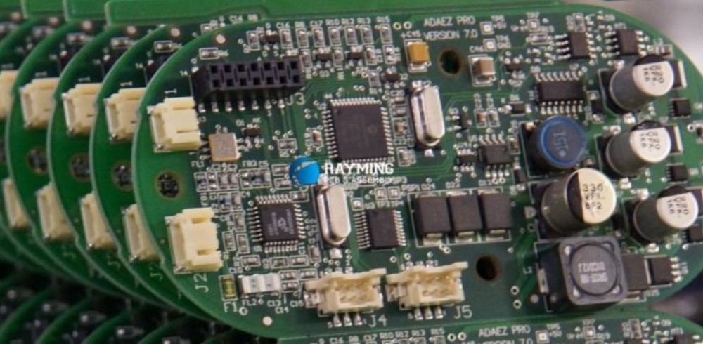
Multilayer
Multilayer PCBs consist of alternating copper and insulating substrate layers laminated together to form complex boards capable of high component densities. Connection between layers are made with plated through holes called vias. High-end complex boards may contain dozens of layers.
PCB Design and Layout
The layout and routing of traces across the PCB is a complex design process aided by specialized PCB design software. Some key layout guidelines and considerations include:
- Following established design rules for trace widths, hole sizes, spacings, etc.
- Minimizing trace lengths for critical signals
- Providing adequate ground planes and power distribution
- Allowing room for component placements and wire routing
- Considering manufacturability and ease of assembly
- Incorporating test points for validation
- Accommodating mating connectors and interfaces
Good PCB layout is critical to achieving proper circuit performance and a quality board build.
PCB Manufacturing Process
Once the board has been designed, it moves into a lengthy fabrication process to turn the design into a physical board:
Data Preparation
The PCB layout data must first be converted into manufacturing data such as phototools drawings, drill tables, and layer images.
Panelization
Multiple PCB designs are arranged and grouped together on larger panels to optimize manufacturing efficiency.
Lamination
Sheets of copper foil and substrate material are stacked and glue together under heat and pressure to form a board panel containing many PCB designs.
Drilling
The panel is precision drilled to create holes for component leads to pass through. High speed CNC drills create thousands of holes per panel.
Surface Processing
The panel goes through multiple chemical processes to pattern the copper layers and apply surface finish. This involves steps such as photoresist application, exposure, etching, stripping, and more.
Solder Masking
A solder mask coating is applied and areas requiring solder exposed. Screen printing, inkjet, and various methods may be used for solder masking.
Legend Printing
Printed legends and markings are added to the panel for labeling, logos, board information, etc. This aids assembly and troubleshooting.
Final Testing
Electrical testing validates continuity of connections and looks for manufacturing faults on the panel. Testing may also include parameters like impedance, leakage, etc.
Depanelization
Individual PCB designs are routed or diced out of the larger panelization resulting in the finished boards.
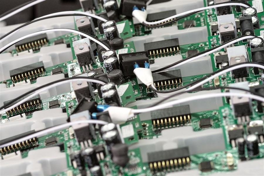
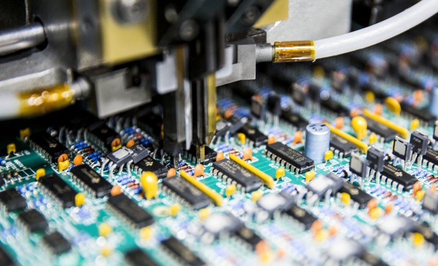
PCB Assembly and Component Mounting
Once fabricated, PCBs move into assembly where electronic components are soldered onto the boards. Some methods for attaching components include:
- Through-hole mounting – Component leads are inserted through holes in the PCB and soldered to pads on the other side to connect the component.
- Surface mount technology (SMT) – Components are soldered directly onto the surface of the PCB without leads passing through holes. Enables higher density.
- Chip-on-board (COB) – Silicon chips are directly mounted onto the PCB. Bonded with conductive adhesive or soldered.
- Press-fit – Components with pins are pressed into slightly smaller plated through holes for a mechanical and electrical connection.
PCB assembly facilities use automated pick and place machines and soldering systems to efficiently assemble boards.
PCB Design Software
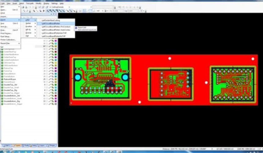
There are a number of software packages available for every stage of the PCB design and manufacturing process:
- Schematic capture – Create circuit schematics showing components connections
- PCB Layout/Routing – Design 2D/3D board layouts and route traces
- Simulation/Analysis – Simulate, verify, and analyze board circuitry
- Library Tools – Generate component symbols and footprints
- Manufacturing Output – Convert data into manufacturing formats like Gerber files
Popular options include Eagle, OrCAD, Altium, KiCad, Solidworks, and more.
Applications of Printed Circuit Boards
Due to their versatility, PCBs are found in nearly every electronics device and system including:
- Computers and Servers
- Mobile Devices
- Telecommunications Equipment
- Automotive Electronics
- Consumer Appliances
- Medical Instruments
- Industrial Electronics
- Military Systems
- Space Systems
Any application requiring compact and reliable circuitry can benefit from the use of printed circuit boards. They enable automation and high volume manufacturing.
Advantages of Using PCBs
Some key advantages of using PCBs over point-to-point wiring or breadboards include:
- Reliability – Soldered and plated connections are very reliable vs. loose wires and contacts.
- Compactness – PCBs allow for much higher component densities.
- Efficiency – Automated assembly is fast and efficient. Lower production costs.
- Serviceability – Consistent construction aids maintenance and repair work.
- Reproducibility – PCB layouts and documentation make replication much easier.
- Customization – PCBs can be designed for specific applications as needed.
- Upgradability – PCBs allow components to be easily changed without rewiring.
- Heat Dissipation – PCB substrate materials conduct heat well aiding cooling.
Clearly, PCBs confer numerous advantages that have solidified them as the electronics packaging technology of choice for modern electronic systems and devices.
Disadvantages of PCBs
PCBs do have some disadvantages and limitations including:
- Initial design/setup costs may be high
- Fabrication and assembly requires significant infrastructure
- Repairing faults not easy without complete schematics
- Traces limited in length, width and current carrying capacity
- Heat dissipation constraints at higher power levels
- Testing and debugging requires specialized tools
- Skilled engineering resources required for design work
Frequently Asked Questions
Here are some common questions about printed circuit boards:
How are components held onto a PCB?
Components are typically soldered onto a PCB’s surface mount pads or through holes. Some components use socket connectors or are press-fit. Adhesives or mechanical means may also be employed.
What are some key metrics used to characterize PCBs?
Trace width/clearance, number of layers, board thickness, maximum frequency, impedance, dielectric constant, component density, board size, etc.
What file formats are used for PCB layout data?
Common formats include Gerber, DXF, ODB++, IPC-2581, STEP, and PDF. These contain layer images, drill data, netlists, etc.
Can PCBs be repaired or reworked?
Yes, it is possible to repair faults by tracing opens/shorts, replacing components, splicing traces, jumper wiring, etc. Reworking methods include soldering, de-soldering, and conductive epoxy.
How environmentally friendly are PCB manufacturing processes?
Many traditional PCB processes use toxic chemicals and generate hazardous waste. Greener options are being adopted such as aqueous processes. Proper recycling also helps minimize environmental impact.
What inspection techniques are used to validate PCB quality?
Automated optical inspection (AOI) and x-ray imaging are commonly used. Testing includes in-circuit tests, flying probe tests, boundary scans, etc.
Conclusion
In conclusion, the printed circuit board is an indispensable core component of modern electronics, enabling the complex circuitry and dense packaging required in advanced devices and systems. While early PCBs were simple single or double sided boards, technology advancements have enabled multilayer boards with thousands of components. The design, fabrication, assembly, and testing of PCBs is a complex endeavor calling upon expertise spanning many technical disciplines. With electronics proliferating into every facet of life, high quality and reliable PCBs will continue to provide the foundational building block for these vital technologies.


Leave a Reply