
Introduction
Vias are plated through holes in printed circuit boards (PCBs) that provide electrical connections between different layers in the board. There are several types of vias, and some are designed to not be visible from the outside of the PCB. In this article, we will discuss the different types of vias and which ones are typically hidden inside the PCB.
Types of Vias
There are three main types of vias:
Through Hole Vias
- Go completely through the PCB from top to bottom
- Drilled holes are plated to make electrical connections
- Visible on top and bottom of PCB
Blind Vias
- Connect an outer layer to one or more inner layers
- Not visible on the opposite side of the PCB
- Allow more routing flexibility
Buried Vias
- Connect two or more inner layers of the PCB
- Not visible from either side of the PCB
- Used to route signals between internal layers
Out of these via types, buried vias are not visible from either side of the PCB. Blind vias may be visible on one side. Through hole vias are visible from both sides.
Why Use Buried Vias?
There are several reasons to use buried vias that are hidden inside the PCB:
- Reduce clutter on outer layers – Keeping vias on inner layers simplifies routing and component placement on outer layers.
- Improve signal integrity – Shorter routing paths by skipping outer layers can maintain signal quality.
- Increase density – Buried vias consume no real estate on outer layers, allowing higher component density.
- Enhance aesthetics – No visible vias makes for a cleaner, more appealing PCB.
When are Buried Vias Used?
Here are some typical situations where buried vias are beneficial:
Connecting Ground/Power Planes
Buried vias are commonly used to stitch together ground and power planes on inner layers. This provides low impedance connections while keeping the outer layers free of clutter.
IC and BGA Fanout
Routing signals from high density IC packages like BGAs is easier using buried vias to fan out signals between inner layers. This maximizes routing channels on outer layers.
RF Circuits
In RF designs, buried vias can be placed strategically to provide shielding and minimize signal interference issues.
Multi-Layer Boards
Boards with 4, 6, 8, or more layers provide opportunity to route signals internally with buried vias.
High Density Designs
When PCB real estate is at a premium, buried vias help maximize component placement space on outer layers.
Challenges of Using Buried Vias

However, there are some difficulties posed by using buried vias:
- Difficult debugging – Lack of physical access makes probing buried connections impractical.
- Complex manufacturing – Plating deeply buried vias requires advanced processes, impacting cost.
- Thermal issues – Buried vias have limited ability to conduct heat, which must be considered.
- Testing limitations – It is harder to directly test buried connections. Test points may need to be routed to outer layers.
Design Considerations
Here are some guidelines to follow when incorporating buried vias in your PCB design:
- Minimize buried via depth and aspect ratio to aid plating quality.
- Access some buried connections with test points on outer layers.
- Ensure adequate thermal relief vias are present for inner layer planes.
- Model effects on impedance, EMI, and signal integrity.
- Follow any special buried via design rules from your board fabrication shop.
- Use blind/buried vias in moderation, balancing benefits with debuggability.
Summary
- Buried vias provide electrical connections between inner layers of multi-layer PCBs.
- They are not visible from either side of the completed board.
- Benefits include reduced clutter, improved signal integrity, and higher density.
- Use is recommended for ground/power planes, BGA fanout, RF boards, and dense designs.
- Challenges include difficult debugging, thermal issues, and testing limitations.
- Following buried via design guidelines will ensure successful implementation.
Frequently Asked Questions
What are some of the disadvantages of using buried vias?
Some potential disadvantages of using buried vias include:
- Difficulty probing or debugging internal connections
- Potential for creating thermal issues or “hot spots” inside the PCB
- More complex PCB fabrication process required
- Potential reliability issues over time due to plating issues
- Limited ability to visually inspect buried connections
- Increased cost compared to standard through-hole vias
- Challenging to validate electrical performance of buried connections
In what types of circuit boards are buried vias most commonly used?
Buried vias are most commonly used in:
- High density interconnect (HDI) PCBs
- Multilayer boards with 4 or more layers
- High frequency radio frequency (RF) circuit boards
- Boards with components requiring high pin counts and routing density like BGAs
- Low noise analog circuit boards where shielding is desired
How can buried vias be tested if they are not accessible from the surface?
While direct physical probing of buried vias is difficult, there are ways to test them:
- Test points can be routed from buried connections to test pads on outer layers
- Continuity testing using a bed-of-nails fixture applies pressure to test pads on both sides
- Flying probe testers can make contact with test points on outer layers
- Automated optical inspection (AOI) looks for defects in plated holes
- Cross-sectioning involves cutting test coupons and viewing buried connections under a microscope
- Electrical testing validates functionality despite lack of physical access
What considerations are important when designing buried vias?
Some key buried via design considerations include:
- Minimize buried via depth and aspect ratio for reliable plating
- Follow fabrication shop’s design rules for spacing, annular rings, etc
- Watch for thermal heat dissipation issues and provide thermal relief as needed
- Model effects on signal integrity, impedance control, EMI
- Include test points on outer layers to facilitate testing
- Use blind/buried vias in moderation to aid debuggability
- Ensure adequate process margin on fabrication tolerances
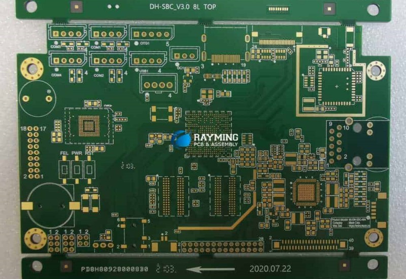
How can you determine if a PCB contains buried vias by looking at it?
It is often impossible to conclusively identify buried vias by visual inspection alone. However, some signs that likely indicate buried vias include:
- Fewer visible vias than expected based on circuit complexity
- Presence of many blind or microvias on outer layers
- High density of traces and components on outer layers
- Noticeable skip vias with no clear routing path on outer layers
- Blocks of copper on inner layers visible through translucent FR4
- Design notes or indicators on PCB mentioning buried vias
- Knowledge that PCB technology supports buried vias
- Specifications or product brief mentions buried vias
While not definitive proof, these factors suggest buried vias are being used to maximize routing density. The only sure way to verify is cross-sectioning or asking the designer directly!


Leave a Reply