Introduction
Printed circuit boards (PCBs) are integral components of most electronic devices. They provide the physical platform to mount and interconnect electronic components using conductive copper tracks. To connect different layers in a multilayer PCB, vertical interconnects called vias are used. The two main types of vias used in PCBs are microvias and buried vias. While both serve the purpose of interlayer connections, they have distinct characteristics, advantages, and limitations. This article will explore the key differences between microvias and buried vias to provide electronics designers and manufacturers a comprehensive understanding of their applications.
What is a Microvia?
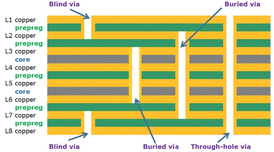
A microvia is a small via with a diameter typically less than 150 μm (or 0.15 mm) used to interconnect two or more adjacent layers in a PCB. The relevant IPC standard IPC-2226 defines a microvia as a laser-drilled blind via with a diameter less than 0.15 mm. The most common microvia diameter range used is 50 μm to 150 μm.
Microvias are fabricated by laser drilling and metallization to create a conductive barrel connecting the layers. They allow routing high-density interconnections between layers, especially in multilayer boards with high component densities. Microvias occupy less space than through-hole vias due to their small diameter. This enables greater wiring densities in the board.
Some key properties and advantages of microvias:
- Small diameter, usually 50-150 μm.
- Used to interconnect 2-3 adjacent layers.
- Allow high-density routing between layers.
- Require laser drilling and metallization.
- Lower fabrication cost than complex blind/buried vias.
Microvias are well-suited for linking together the surface layers of high density PCBs. However, they are limited to adjacent layer connections only. For non-adjacent layers, other via types are used.
What is a Buried Via?
A buried via is an interconnect between internal non-adjacent layers of a multilayer PCB. They are formed by drilling and plating through a core layer. Once the core is laminated between other dielectric build-up layers, the via becomes “buried” internally.
Buried vias can connect between any two or more non-adjacent inner layers in a PCB. For instance, they can link the 2nd and 5th layer in a 6 layer board. The dielectric build-up layers electrically isolate the buried via from the outer board layers.
Key characteristics of buried vias:
- Can interconnect any non-adjacent inner layers.
- Formed by drilling/plating in the core layers.
- Require complex lamination process to bury the via.
- Large diameters, typically 300-400 μm.
- Allows routing between non-adjacent inner layers.
Buried vias enable indirect layer connections where routing channels are blocked on adjacent layers. They also reduce the need for stub traces in high layer count boards. However, the fabrication process is more complex than microvias.
Key Differences between Microvias and Buried Vias
| Parameter | Microvia | Buried Via |
|---|---|---|
| Definition | Blind via connecting 2-3 adjacent layers | Via connecting any non-adjacent inner layers |
| Diameter range | 50 – 150 μm | 300 – 400 μm |
| Fabrication method | Laser drilled and metallized | Mechanically drilled/plated in core |
| Layer connection | Adjacent layers only | Any non-adjacent inner layers |
| Routing density | Allows high-density routing between layers | Low density, occupies more space |
| Fabrication complexity | Relatively simple | Complex lamination process |
| Cost | Lower | Higher due to complexity |
In summary, the major differences are:
- Diameter size – Microvias are much smaller in diameter than buried vias.
- Layer connection – Microvias connect adjacent layers, buried vias connect non-adjacent inner layers.
- Routing density – Microvias allow dense routing due to their compact footprint. Buried vias are larger and take more space.
- Fabrication – Microvias only require laser drilling while buried vias need complex core layer lamination.
- Cost – Microvias are cheaper to fabricate than buried vias.
PCB Stackup Configurations using Microvias and Buried Vias
Based on their distinct capabilities, microvias and buried vias can be strategically used in different zones of the PCB stackup. Some examples are:
4-layer board with microvias
In a 4-layer PCB, microvias can be used to interconnect the two outer layer pairs. Through-hole vias connect between the inner and outer layers.
6-layer board with microvias and buried vias
Here microvias link the adjacent outer layers while buried vias connect the inner layers. The buried and blind/hidden vias provide routing between non-adjacent layers.
10-layer board with microvia HDI and complex buried vias
Advanced 10+ layer HDI boards can use microvias in the high-density buildup layers along with staggered vias/buried vias in the inner core. This allows maximum routing flexibility.
The stackup configuration will depend on the board’s layer count, routing density requirements, layer connections needed, and fabrication capabilities.
Typical PCB Applications using Microvias and Buried Vias
Microvias are commonly found in:
- High density interconnect (HDI) PCBs
- RF/microwave circuit boards
- LED PCBs
- Flex/rigid-flex PCBs
Buried vias are used in:
- High layer count >10 layer boards
- Complex multilayer boards
- PCBs requiring connections between inner layers
- EMI shielding applications
High performance digital circuits like CPUs, GPUs, FPGAs use dense HDI and complex via structures with both buried and stacked microvias. Cost-driven consumer electronics employ mostly lower layer counts with microvias.
Fabrication and Testing Challenges
Microvia challenges:
- Achieving reliable metallization and plating inside small microvias.
- Preventing microvia stub failures. Stubs can cause impedance discontinuities.
- Testing for defects and ensuring reliability of microvias. X-ray inspection is used.
- Stacked microvias require sequential laser drilling and alignment.
Buried via challenges:
- Accurate registration and drilling of vias in multilayer core.
- Preventing buried via failures like opens or shorts between layers.
- Verifying connections of buried vias between inner layers.
- Fabrication process control is critical.
Modern PCB manufacturers use advanced drilling, metallization, and lamination processes to fabricate complex via structures reliably. Automated optical and X-ray inspection and electrical testing help ensure quality standards are achieved.
Summary
In summary, here are the key takeaways:
- Microvias – Small, laser-drilled vias connecting adjacent layers. Allow high-density routing. Lower cost.
- Buried vias – Large mechanically drilled vias connecting non-adjacent inner layers. Provide flexibility in routing channels. Higher fabrication complexity and cost.
- Microvias are used for surface layer interconnects while buried vias link up inner layers in multilayer boards.
- Stackup design, layer count, routing density and design rules determine the types of vias used.
- Fabrication accuracy and testing is crucial for reliable via interconnections.
Both microvias and buried vias fulfil important roles in PCB design. Understanding their differences allows engineers to apply the appropriate via structure and density for their application requirements.
Frequently Asked Questions
What are the typical fabrication tolerances for microvias and buried vias?
For microvias, diameter tolerance is typically ±10% and positional accuracy around 25 μm. Buried vias have larger tolerances – diameter ±25% and position 50-100 μm.
Can stacked vias be used instead of buried vias?
Yes, stacked/staggered microvias provide an alternative to connect non-adjacent layers without using large buried vias. But fabrication complexity increases.
Do microvias affect signal integrity at high speeds?
At very high frequencies > 5GHz, if not designed properly, microvias can cause discontinuities. Backdrilling stubs, keeping via lengths short, and matching impedance help alleviate issues.
Are buried vias only for inner layers?
No. It is also possible to design buried vias between outer conductive layers by using blind/buried vias in the outer layers. But this increases fabrication complexity.
Can microvias connect 4 or more layers?
Connecting more than 2-3 adjacent layers with a single microvia is challenging. But laser drilling and metallizing a daisy chain of stacked microvias allows connecting multiple layers if designed properly.


Leave a Reply