Introduction to Buried Vias
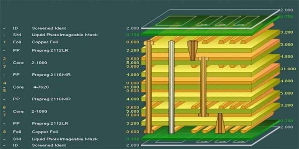
Buried vias are a type of via connection used in printed circuit boards (PCBs) to connect different layers of a multilayer PCB. Vias are plated through holes that allow traces on different layers to be electrically connected.
In a typical via, the hole is plated through from the top layer to the bottom layer of the PCB. The via barrel is then filled with solder mask, leaving the via pads exposed on the outer layers for component connections.
A buried via differs in that it does not connect to the outer layers. Instead, it only connects internal layers of the PCB. The buried via barrel and pads are completely covered by solder mask on the outer layers.
Advantages of Buried Vias
There are several benefits to using buried vias:
- Frees up space on outer layers – Since buried vias do not connect to the outer layers, they do not use up space on the top or bottom layers for via pads. This leaves more space available for routing traces and placing components.
- Allows higher component density – Without via pads taking up space on the surface, components can be placed closer together. This allows for more compact PCB layouts overall.
- Reduces drilling costs – Fewer through-hole vias means lower drilling costs for the PCB fabrication shop. Buried vias only need to drill down to the intermediate layer connections.
- Improves signal integrity – By keeping signals on inner layers, buried vias can reduce electromagnetic interference issues and cross talk between signals. The outer ground planes help shield signals traversing buried vias.
- Simplifies high-speed routing – Sensitive high-speed traces can be routed on inner layers and avoid discontinuities from surface vias. Buried vias help maintain controlled impedance across layers.
Disadvantages of Buried Vias
The main disadvantage of using buried vias is reduced repairability and accessibility:
- Difficult probing – Buried vias cannot be physically accessed without removing solder mask. This complicates debugging and probing of internal layer signals.
- Challenging rework – If a buried via connection is faulty, it is very difficult to access and replace. Often the entire PCB must be scrapped.
- Additional fabrication steps – The PCB fab must process steps to fill the buried via holes and cover them with solder mask. This increases time and cost.
- Not suitable for prototyping – Buried vias cannot easily be hand-soldered. They are only practical for higher volume PCB production.
Where are Buried Vias Used?
Buried vias tend to be used in more complex, high density PCB designs where space is tight and signal performance is critical. Typical applications include:
- High speed digital circuits – Buried vias maintain uniform impedance for tightly routed signals traversing PCB layers. This is key in computing applications.
- RF/microwave boards – Keeping critical RF traces on inner layers avoids interference and losses. Buried vias minimize discontinuities.
- Mixed signal boards – Separating analog and digital domains across layers while linking them with buried vias enhances signal integrity.
- Multi-layer boards – Complex boards with 6+ layers depend heavily on buried vias for inner layer connectivity. Their small size and layer flexibility is advantageous.
- High pin count BGAs – Dense component packages require many interconnects between layers. Buried vias conserve real estate for escape routing.
- LED lighting PCBs – Buried vias integrate the tight layouts required for high density LEDs and drivers. Heat management is also improved.
In general, any PCB that requires optimized space usage, tight clearances, controlled impedances, or separation of critical nodes will benefit from exploiting buried vias. Their buried nature avoids cluttering the outer layers.
How are Buried Vias Constructed?
Constructing buried vias requires a multilayer board fabrication process capable of making interlayer connections within the PCB stackup. There are three main techniques used:
Laser Drilled Vias
Similar to through-hole vias, a laser is used to ablate a hole through the layers to be connected. The hole is then plated with copper to form the electrical connection between layers:
- Allows drilling vias after layers are laminated together. Vias can be placed anywhere needed.
- High accuracy systems allow small via holes and precise location.
- Limitations in aspect ratio of depth to width of hole.
- Relatively slower process compared to other methods.
Microvias
Microvias are small vias produced photolithographically without mechanical drilling. The vias are plated up sequentially between each layer:
- Very small diameter vias are possible, down to 0.005” (0.13mm) or less.
- Allows very high via densities with tight pitch.
- Allows stacking vias vertically for interlayer connections.
- Limited by number of lamination cycles. More cycles increase fabrication time and cost.
Buried Plated Through-Holes
Holes are mechanically drilled, plated, and then buried:
- Process resembles standard plated through hole vias.
- Very low cost compared to laser or microvia processes.
- Capability depends on PCB fab equipment maximum hole depth and aspect ratio.
Via Backfilling and Capping
For buried vias made by any process, the hole is backfilled with epoxy resin toplug the hole between the desired layer connections:
| Via Process | Aspect Ratio | Minimum Size | Density | Cost |
|---|---|---|---|---|
| Laser Drilled | Medium | 0.002” | Medium | Medium |
| Microvia | High | 0.0005” | High | High |
| Buried PTH | Low | 0.010” | Low | Low |
Backfilling yields a flat surface and eliminates voids inside the board. The entire via barrel is then masked with solder mask on the outer layers to fully isolate and insulate the buried via.
Design Rules for Buried Vias
To effectively implement buried vias in a design, certain rules and limitations must be followed:
- Via width – The drilled hole size must allow for adequate plating thickness based on the via depth and process limitations.
- Capture pads – Laser drilled buried vias require capture pads on connecting layers for reliable plating.
- Spacing – Close spacing increases fabrication difficulty due to limited laser beam diameter or drill bit length.
- Reliability – Aspect ratio and hole fill impact via reliability. Keep drill depth below 5:1 ratio for best results.
- Layers – Laser drilling can typically reach 10+ layers. Other processes may be limited to fewer layers.
- Registration – Tight tolerance on laser systems allows smaller capture pads. Larger pads needed for drilled holes.
- Densities – Microvias enable very high densities. Other processes are limited by minimum spacing rules.
- Stacking – Some processes allow stacking vias vertically to reach multiple layers.
Following the PCB manufacturer’s specific buried via capabilities and design rules is key to a successful implementation. Their process rules will determine the optimal buried via approach.
Buried Vias vs Blind/Staggered Vias
There are some similarities between buried vias and related via structures like blind and staggered vias:
- Blind vias – Connect an outer layer to one or more inner layers, but do not go completely through the PCB.
- Staggered vias – Electrically connect two different layers using two separate drilled holes that line up on pads.
The key difference versus buried vias is that blind/staggered vias leave one side fully accessible for probing or rework. Buried vias have both sides covered.
In some cases, a staggered viaapproach may be preferable if accessibility to intermediatelayers is desired. Buried vias provide the highest degree of layerisolation.
Challenges of Designing with Buried Vias
Despite their advantages, buried vias also impose some design challenges:
- Lack of accessibility as noted previously makes debugging difficult. May require specialized microprobing equipment.
- Simulating performance is dependent on CAD tools accurately modeling via behavior and interactions between layers. This is improving but still complex.
- Tuning buried via architectures for target impedance and noise containment requires precise modeling and testing.
- Skew between signals passing through differing via structures must be accounted for in high speed designs.
- Fabrication processes introduce tolerances on via placement, size, hole fill, etc. These variations can impact signal integrity if not designed with adequate margin.
- Quality control and testing for buried vias is largely dependent on indirect methods like x-ray imaging or external measurements. Direct inspection is not possible.
For these reasons, buried via PCBs require a rigorous design validation process including simulation, prototyping, and performance testing to verify the design intent is achieved within the needed tolerances.
Frequently Asked Questions
What are some key terms related to buried vias?
Here are some key terms used when discussing buried vias:
- Via – A plated through hole used to connect layers of a PCB.
- Buried Via – A via that connects internal layers without going through to the outer surfaces.
- Blind Via – A via that connects an outer layer to one or more internal layers only.
- Through Via – A via that extends through the entire PCB stackup to connect the top and bottom outer layers.
- Microvia – A mechanically drilled via typically less than 0.005″ in diameter. Allows high density.
- HDI PCB – High Density Interconnect PCB using microvias. Enables compact interconnects.
- Capture Pad – Metal pad that makes contact with plated barrel of a buried via. Necessary for plating process.
- Via Tenting – Covering a via completely with solder mask to isolate it or make it “buried”.
How do buried vias affect the PCB fabrication process?
Adding buried vias to a design impacts the PCB fabrication in several ways:
- Additional drilling may be required to form the vias after layer lamination. This slows the process.
- Precise depth control of drilled holes is critical. This may require specialized equipment.
- For microvias, additional lithographic steps are needed to build up connections layer by layer.
- Buried vias require precision hole filling and planarization processes to avoid voids.
- Thicker boards require tighter process controls to achieve target hole depths and aspect ratios.
- Solder mask application steps must uniformly cover buried vias while leaving other vias clear.
- Testing and inspection requirements increase due to lack of access to buried interconnects.
Overall, fabricating boards with buried vias is slower, more complex, and costs more compared to standard through-hole via processes. The fabrication shop needs the technical capabilities to handle buried via demands.
What are considerations for buried via location?
Some guidelines for optimizing buried via placement:
- Place near signal via transitions between layers to limit stub lengths.
- Avoid placing under BGA pads which limits solder void inspection. Offset slightly if possible.
- Leave adequate clearance between buried via capture pads and inner layer traces.
- Dense surface mount regions are good candidates for diverting connections internally.
- Ensure good registration between layers when interconnecting points on different layers.
- Plan around limitations on proximity between adjacent buried vias due to hole spacing requirements.
- It can be helpful to align buried vias in rows/columns to simplify design restrictions.
- Balancing buried via assignments between layers helps distribute density and fabrication stress.
How are buried vias modeled in PCB design software?
Buried vias can be modeled in various ways in PCB design tools:
- As a standard via object with properties set to tent/mask both outer layers.
- As a blind/buried via object connecting the desired internal layers.
- With multiple separate blind via objects stacked vertically.
- As a pin-pair through an empty cutout to mimic the layer transitions.
The modeled via structure must represent the actual fabricated via technology for accurate simulation. This may require multiple pins or objects to create an electrically equivalent model. Advanced tools provide specific buried via modeling features to capture all the 3D effects accurately.
How are buried vias tested and inspected?
Since buried vias have limited physical access, specialized techniques must be used:
- X-ray imaging can detect voids in via filling and measure registration between layers.
- Cross-sectioning uses microscope inspection of a cut cross-section to reveal the internal structure.
- Microprobing instruments can probe internal layers through prepared pad exposures or direct layer access.
- Electrical testing checks for shorts, opens, and interlayer connectivity issues.
- External measurements characterize electrical performance like impedance, attenuation, and propagation delay.
- Pattern accuracy inspection validates capture pad alignment, spacing, and metallization defects.
- Process monitors, like microsections or x-rays, on coupon boards help dial in equipment parameters.
Though challenging, adequate buried via inspection methods combined with simulation, modeling, prototyping, and design reviews help mitigate risks and improve yields.


Leave a Reply