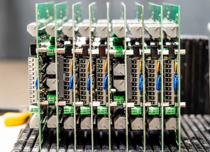
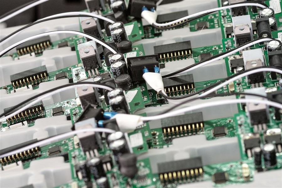
Vias are metalized holes that allow connections between different layers of a printed circuit board (PCB). They provide vertical interconnects to route signals between layers and connect surface mounted components to inner layer traces. While essential for routing and connectivity, vias also impact the overall cost of PCB fabrication and assembly. In this article, we’ll explore how vias affect PCB cost and discuss ways to optimize via design to balance functionality and affordability.
How vias impact PCB fabrication cost
During PCB fabrication, vias are formed by drilling holes and then plating the walls with copper to create the electrical connection. The main PCB fabrication costs associated with vias are:
- Drilling – The via holes must be precisely drilled, typically with mechanical drilling or laser drilling machines. More vias require more drilling time and tooling usage.
- Plating – Electroless and/or electroplating is used to coat the drilled via holes with copper. More plated hole surface area requires greater plating chemical usage.
- Testing – Each via needs to be tested for continuity and isolation after fabrication. More vias require more test points and longer test time.
- Yield – Vias create potential failure points during fabrication. Higher via counts can decrease yield due to defects like opens or shorts.
- Handling – Smaller vias and those with thicker boards require specialized drill bits. Tight via pitches may also require custom fixturing.
- Depanelization – Vias along board edges require specialized breakout tooling after panelization. Higher via counts near board edges drive up depanelization costs.
In summary, higher via quantities directly increase material, labor, tooling and test costs during PCB fabrication. As a rough estimate, each additional 100 vias per square inch of board area adds approximately 5% to the bare board fabrication cost.
How vias impact PCB assembly cost
Vias affect the process of assembling components onto the PCB in the following ways:
- Solder filling – Each via acts as a “through hole” that needs to be filled with solder, adding material cost.
- Inspection – More vias require additional automated optical inspection (AOI) programming and run-time for solder fill validation.
- Rework – Unfilled or partially filled vias may require rework adding additional process steps.
- Routing congestion – An abundance of vias can create congested routing channels, forcing components to be placed less optimally.
- Thermal relief – Vias are thermal conductors and sinks. Excessive vias under components may impact soldering process windows.
- Signal integrity – Poorly designed via stubs and excess capacitance can degrade high speed signals. Simulation and testing costs go up.
- Board handling – High via edge densities can lead to breakage during depanelization or handling.
In general, above 200-300 vias per square inch, assembly costs start to rise disproportionately due to the factors mentioned above. The relationship is not linear but accelerates with higher via densities.
How to reduce PCB cost from vias
While vias are essential interconnects in a PCB design, there are ways to minimize their cost impact through optimization:
Layer count
Adding PCB layers enables more routing channels and reduces the number of vias required. Though layer count increases base fabrication cost, the tradeoff often reduces the total cost by lowering via quantities. 4-6 layers is a typical range for balancing cost.
Via distribution
Spreading vias evenly across the PCB avoids locally high concentrations that drive cost exponentially. Common practices include:
- Set maximum vias per area
- Configure autorouters to distribute vias
- Manually route to spread out vias
Via size/shape
Using the minimum viable via size saves on drilling time and plating costs:
- 0.3-0.35mm dia. for signal vias
- 0.2-0.25mm dia. for IC vias
- Slotted or buried vias when possible
Build-up vias
Laser drilled microvias (0.1-0.15mm) in build-up layers reduce the number of through-hole vias. This shifts cost from expensive drilling/plating to lower cost processes.
Plugged vias
Plugging unused through-hole sites with masking or filling can eliminate unneeded plating and drill cycles.
Panel utilization
Grouping boards to maximize panel space reduces the number of tooling hits per board. Careful placement of vias relative to tooling rails and breakouts also helps.
Design rules
Establishing and following rules for via quantity, size, spacing, etc. prevents uncontrolled proliferation. Exceptions can be allowed but controlled through design reviews.
Example impact on a sample PCB

To illustrate the cost dynamics, let’s compare two hypothetical PCB designs:
Design A
- 4 layer board
- Board dimensions: 100 x 100 mm
- 500 components with 2000 pins
- Conservative routing with 3000 vias
Design B
- 4 layer board
- Board dimensions: 100 x 100 mm
- 500 components with 2000 pins
- Optimized routing with 1000 vias
By reducing the via count by 2X, here is the estimated cost savings for Design B:
| Cost Factor | Savings |
|---|---|
| Drilling time | 20% |
| Plating chemicals | 15% |
| Test points | 30% |
| Rework | 10% |
| AOI programming | 5% |
| Total Saving | ~15% |
This simplified example demonstrates the potential production cost benefits from via optimization, which can add up to substantial savings. The results will vary based on design complexity, volume, and capabilities of the PCB fabricator and assembler.
Frequently asked questions
How many vias can you have before it gets expensive?
As a rough guideline, more than 200-300 vias per square inch will start driving costs higher. However, it depends largely on via size, distribution, and PCB technology. A good practice is to establish design rules and get early feedback from your fabrication partner.
Is there a difference between through-hole and blind/buried vias cost?
Yes, blind and buried vias can be lower cost since they are laser drilled in the inner layers, avoiding more expensive through-hole mechanical drilling. The tradeoff is that blind/buried vias may require additional layers.
Are microvias cheaper than standard vias?
Microvias (below 0.15mm diameter) utilize lower cost laser drilling so they can decrease cost, provided the board shop has compatible capabilities. But they still add surface area for plating and inspection.
How can I estimate the cost of adding more vias?
As a rough estimate, each additional 100 vias per square inch adds about 5% to total PCB fabrication costs. But it’s highly design dependent, so early supplier involvement can provide more accurate guidance.
What are some key things I can do to reduce PCB via costs?
Some best practices are: distribute vias evenly, use the minimum viable size, utilize blind/buried vias, reduce layers if possible, maximize panel utilization, establish and follow design rules.
What is a viable via size I should target?
For signal routing on outer layers, 0.3-0.35mm diameter vias offer a good balance of manufacturability and cost. For high density interconnects, 0.2-0.25mm diameters can be feasible with tighter design rules.
Conclusion
Vias are critical for routing PCB designs but also have a direct correlation to manufacturing costs. Each additional via adds costs for drilling, plating, inspection, potential yield loss and assembly rework. Careful attention to via quantity, distribution, size and fabrication process can help optimize cost. With a well-designed PCB stackup and layout that minimizes unneeded vias, it is possible to balance connectivity needs with overall affordability.


Leave a Reply