Introduction
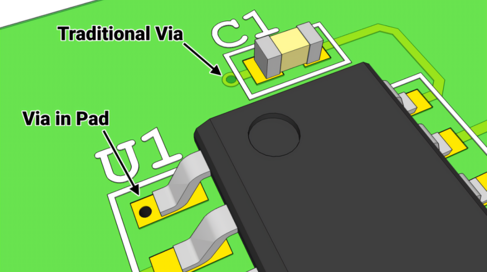
When designing printed circuit boards (PCBs), vias and pads are two important features that enable connections between different layers of the board. A via is a plated through hole that connects two or more layers in the PCB, while a pad is the metal surface onto which components are soldered. A common question that arises during PCB design is whether it is acceptable or advisable to place vias on pads. In this article, we will explore the factors involved in deciding if and when you can or should put vias on pads.
Benefits of Putting Vias on Pads
There are a few potential benefits to placing vias on pads:
Saves Space
Putting a via on a pad conserves real estate on the PCB. Combining the two features into one area reduces the amount of space that must be dedicated to interconnects. This can allow for a more compact layout.
Reduces Drilling Costs
Since you are using one drilled hole for both the via and the pad, it eliminates the need to drill an additional hole specifically for a via. Less drilling equates to lower fabrication costs.
Simplifies Routing
Having a via directly on the pad simplifies trace routing. The via provides immediate access to another layer without having to route a trace across the surface of the board to connect the pad to a separate via.
Drawbacks of Vias on Pads
However, there are also some disadvantages that should be considered when deciding whether or not to put vias on pads:
Reduced Pad Area
The via hole will consume some of the surface area of the pad. This effectively reduces the available area for soldering component leads or connectors to the pad.
Increased Risk of Solder Voids
The presence of the via hole in the pad increases the chances of creating voids when soldering. This occurs because solder can partially or fully fill the via hole, leaving less solder directly on the pad surface.
EMI Concerns
Placing a via hole directly in a ground or power pad can create EMI issues. The hole disrupts optimal current flow across the pad plane surface.
Mechanical Stress Risk
There is higher mechanical stress concentration around the via, which is located in the pad. This can result in cracked pad surfaces.
Redundant Vias
If you already have a via near the pad for routing purposes, adding another via on the pad itself results in redundant vias, increasing cost without significant benefit.
Guidelines for Putting Vias on Pads
Based on the tradeoffs discussed, here are some general guidelines regarding when it may or may not make sense to put vias on pads:
Non-Critical Traces
Use vias on pads for routing non-critical, low current traces. This avoids problems on essential pads like grounds.
SMD Pads
Surface mount pads are generally okay for vias since solder voids are less likely with SMD pads. Avoid vias on through-hole pad connections.
Large Pads
Pads that are relatively large in area to begin with can more easily accommodate vias, since enough pad area remains for soldering.
Power Planes
It’s best to avoid locating vias on power and ground planes. Use dedicated thermal relief pads instead for vias.
Double-Sided Boards
Vias on pads make more sense for double-sided boards where space is extremely constrained. On multilayer boards, routing options are more flexible.
Non-Plated Vias
For pads requiring a via, consider a non-plated via which avoids disruption of the pad surface by solder.
Test First
When in doubt, prototype and test a few boards to confirm via placement on pads does not cause significant soldering or EMI issues.
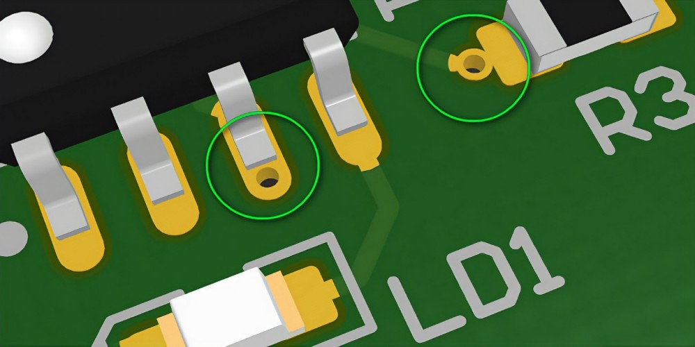
Examples of Vias on Pads
Here are a few examples of appropriate and inadvisable ways to use vias on pads:
Table: Examples of Vias on Pads
| Good Example | Bad Example |
|---|---|
| SMD resistor pad with small via to inner layer | Large via on through-hole connector pad |
| Via on secondary digital logic power pad | Multiple vias on critical ground pad |
| Non-plated via on analog IC power pad | Plated via on large QFP landing pad |
As shown in the table, vias on smaller SMD landing pads, secondary power pads, and non-plated vias on certain pads can potentially be acceptable. But use caution with large vias on through-hole pads, clusters of vias on ground/power planes, and plated vias on large surface mount landing areas.
Alternatives to Vias on Pads
If best practices indicate you should avoid placing a via on a particular pad, here are some alternative options to consider:
- Route a trace from the pad to a nearby via.
- For ground/power planes, use thermal relief pads tied to the main pad.
- For dense BGA packages, redirect traces so that vias are between pads.
- For high pin count devices, implement routing channels to reduce via overlap on pads.
- Where possible, make use of component layer pads to avoid passing vias through all layers.
Impact of Via-in-Pad Plating
The plating process used for via holes can also be a factor when debating vias on pads. Two main options exist:
Unplated Vias: The via barrel remains unplated. The sides retain the base laminate material. This avoids solder wicking down into the via.
Plated Vias: The via hole is plated with copper, connecting the layers. This allows solder to fully fill the via during reflow.
In general, unplated vias are preferred for via-in-pad applications, since they reduce solder voiding issues versus plated vias. However, unplated vias can present challenges for solder masking within the via.
Summary
- Placing vias on pads can offer some benefits but also has multiple drawbacks to weigh.
- It can be acceptable for less critical traces but avoid for essential pads. Follow guidelines on pad size and non-plated vias.
- Alternatives exist like moving vias adjacent to pads or routing channels between pads.
- When used judiciously based on design constraints, vias on pads can provide efficient routing without compromising soldering or performance.
FAQ
What are the main benefits of putting a via on a pad?
The potential benefits are saving PCB space, reducing drilling costs, and simplifying trace routing since the via is right on the pad location.
When would you want to avoid putting a via on a pad?
Avoid vias on critical ground/power planes, large through-hole component pads, and any pad where solder voids could cause functionality or reliability issues.
Is it okay to put a via on a surface mount pad?
Generally it is acceptable to put vias on smaller surface mount pads since solder voids are less likely compared to through-hole pads. But still follow other guidelines regarding pad size, etc.
What is a good rule of thumb for the ratio of via hole to pad size?
As a general rule, the via diameter should be no larger than 0.5 mm for every 1 mm of pad diameter. This helps ensure adequate remaining pad area.
How does an unplated via differ from a plated via on a pad?
An unplated via leaves the barrel laminate exposed and avoids solder wicking down into the hole. This reduces solder voids but can make solder masking more challenging.


Leave a Reply