Introduction
Printed circuit boards (PCBs) contain vias to provide electrical connections between different layers of the board. Vias are plated-through holes that allow signals to travel in the Z-axis between layers. There are two main types of vias used in PCBs – blind vias and microvias. Both provide interlayer connections but have important differences in their structure, size, fabrication, and applications. This article will compare blind vias and microvias – their definitions, sizes, fabrication processes, pros and cons, and appropriate use cases. Clear understanding of their differences allows for optimal via selection during PCB design to meet performance, cost, and manufacturability requirements.
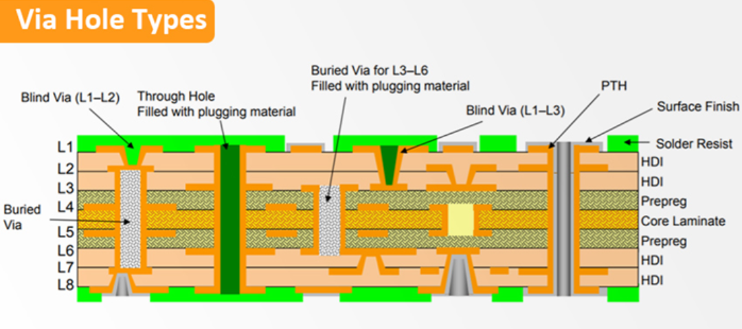
What are Blind Vias?
Blind vias provide connections between some but not all layers of a multilayer PCB. A blind via extends from the outer layer and connects to only one or more inner layers of the board. It does not go through the entire PCB stackup connecting the top and bottom sides. Blind vias are categorized based on the number of layers they connect:
- True blind vias – Connect an outer layer to the first adjacent inner layer. For example, connecting Layer 1 to Layer 2 in a 4 layer board.
- Buried blind vias – Connect an outer layer to an inner layer that is not immediately adjacent to it. For example, connecting Layer 1 to Layer 3 in a 4 layer board.
<p align=”center”> <img src=”blind_via.png” alt=”Blind Via Image” width=”400″> </p>
Figure 1: Examples of true blind and buried blind vias in a multilayer PCB.
Blind vias are most commonly used for the following applications:
- Escape routing – Allow connections from surface mount components that have high density pin patterns and cannot be properly routed on outer layers. The connection is escaped to another layer using a blind via.
- Signal routing – Critical signals can be routed on inner layers to shield them from noise. Blind vias provide access to the inner layer routing.
- Component connections – Components attached to outer layers often require connections to inner layer power or ground planes. Blind vias provide these connections without passing through the entire board.
Some key properties of blind vias:
- Sizes range from 0.2 mm to 0.5 mm or larger if used as thermal vias under heat generating components.
- Require separate drilling and plating steps for each blind via layer connection. Additional processing steps increase fabrication costs.
- Laser drilling can produce small blind vias not achievable with mechanical drilling. Permits higher interconnect densities.
- Well suited for high layer count boards (>6 layers) where multiple separate drilling steps are already required. The incremental cost is low.
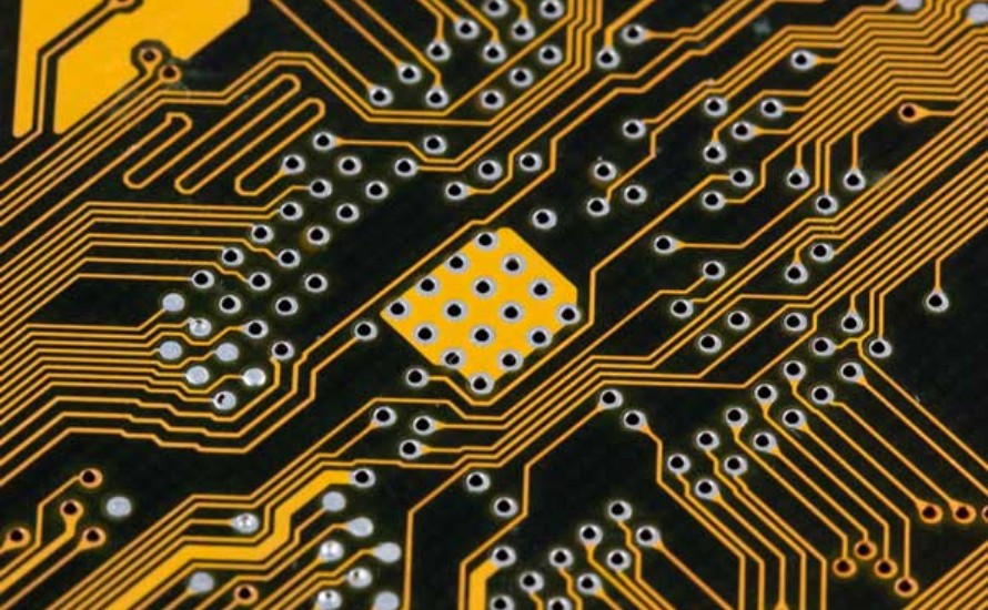
What are Microvias?
Microvias are small vias with diameters less than 0.15 mm (0.006″), connecting two adjacent layers in a PCB. They serve as interlayer connections in high density interconnect (HDI) technology boards. Microvias are laser drilled and typically connect paired adjacent layers as part of a microvia interconnect system:<p align=”center”> <img src=”microvia.png” alt=”Microvia Image” width=”500″> </p>
Figure 2: Microvia structure connecting Layer 1 to Layer 2 pad.
Microvias provide the following benefits:
- Extremely small diameters permit very high connection densities not achievable with standard vias. Allows routing complex ICs with pin pitches under 0.4 mm.
- Short interconnect lengths lower parasitic inductance and capacitance, ideal for high speed signals.
- Fully filled during plating process. No separate hole plugging step required.
- Well suited for assemblies requiring stacked microvias built up across several layers.
Typical microvia applications:
- Flip chip package connections – Microvias under bumped die connect to printed pads. High density connections accommodate fine IC bump pitches.
- IC packages – Used extensively in ball grid array (BGA) and other high pin count packages.
- High speed designs – Short stubs reduce parasitic effects for multi-Gbps signals. Minimizes signal loss and distortion.
- RF/microwave circuits – Provides precise impedance control and low inductance ground vias needed at high frequencies.
- Stacked vias spanning 6-10+ layers to route signals vertically across multilayer boards.
Comparing Blind Via and Microvia Sizes
The most fundamental difference between blind vias and microvias is their size and drilling method used during fabrication:
| Via Type | Drill Method | Typical Size Range |
|---|---|---|
| Blind Via | Mechanical or Laser | 0.20 mm to 0.50+ mm diameter |
| Microvia | Laser Only | 0.05 mm to 0.15 mm diameter |
- Blind vias span a wide range of larger sizes suitable for general routing with lower to moderate interconnect densities.
- Microvias represent the smallest vias fabricated in PCBs to support ultra-fine pitch components and multilayer stacking.
- Blind vias can be mechanically drilled. Microvias require laser drilling to achieve the intricate small features.
Fabrication Process Comparison
Blind vias and microvias also differ significantly in their PCB fabrication sequences involving layer imaging, drilling, and plating:
Blind Vias
Blind via fabrication includes:
- Imaging – Each outer and inner layer is imaged with desired copper patterns. Blind via locations are imaged on respective layers that will interconnect.
- Mechanical Drilling – Drill through the outer layer and into inner layer(s) at blind via locations using mechanical drill bits.
- Laser Drilling – For high density designs, laser drilling provides smaller blind vias than mechanical drills. Performed after mechanical drilling.
- Plating – Electroless copper followed by electrolytic copper to plate the sidewalls of the blind vias.
- Hole Plugging – Blind vias are typically tent plated on their lower connection layer. The holes are filled with epoxy or resin to plug the vias prior to outer layer lamination.
- Outer Layer Lamination – Bonds the outmost circuitized core layer with prepregs and foil to form the finished board. Blind vias have interlayer connections through the partial depth holes.
Microvias
Microvia PCB fabrication involves:
- Layer Imaging – Each conductive layer is imaged to form the circuit traces along with microvia pads. Aligns pads between layers.
- Laser Drilling – Precisely ablates microvia holes through the combined outer and inner layer pads using a laser.
- Plating – Copper is deposited along microvia sidewalls to electrically interconnect the layers. The small holes are completely filled with copper.
- Repeating – Imaging, drilling, and plating repeats to stack microvias across multiple board layers to form a high density interconnect network.
- Outer Layers – Final imaging and lamination of outer layers completes the HDI PCB.
In summary, microvia processing requires additional aligned layer imaging steps and repeated cycles of laser drilling and plating to build vertically interconnected microvia stacks within the PCB. The small microvias are drilled and plated together as a single dense structure.
Pros and Cons Comparison
Blind vias and microvias offer unique advantages and disadvantages based on their size, cost, manufacturability, and performance:
Blind Vias
| Pros | Cons |
|---|---|
| Lower cost than microvias due to conventional drilling | Larger sizes limit routing density versus microvias |
| Well established fabrication process | Multiple drilling/plating steps required for each blind via depth |
| Suitable for moderate density interconnections | Parasitic inductance and capacitance higher than microvias |
| Large variety of sizes tailored to needs | Hole plugging can reduce reliability versus filled microvias |
Microvias
| Pros | Cons |
|---|---|
| Ultra-high interconnect density | Expensive laser drilling and imaging |
| Minimizes parasitic effects | Challenging fabrication process control |
| Improves signal integrity at high speeds | Limited to low loss materials compatible with lasers |
| Filled during plating increases reliability | Generally lower current limits than blind vias |
Comparing Appropriate Use Cases
Based on their characteristic advantages, disadvantages, and capabilities, here are guidelines on effective applications for blind vias and microvias:
Recommended Uses of Blind Vias
- Moderate density routing of surface mount components. 0402 and larger packages.
- Creating access points to internal routing layers.
- Thermal vias under hot components. The larger sizes improve heat dissipation.
- Low to medium complexity boards where microvia stacks are not needed. 2-8 layer designs.
- Cost sensitive applications. Blind vias cost less than microvia processes.
Recommended Uses of Microvias
- Ultra-fine pitch ICs with pitches under 0.4 mm like flip chips or BGAs.
- Networking PCBs with signals over 5 Gbps where low parasitics are critical.
- High speed digital circuits with fast edge rates under 100 ps.
- RF boards operating over 10 GHz requiring excellent impedance control.
- Boards above 8 layers where stacked microvias can simplify vertical interconnections.
- Systems where reliability and performance outweigh PCB fabrication costs.
Summary of Differences
Blind vias and microvias address different PCB interconnect challenges. The key differences are:
| Parameter | Blind Vias | Microvias |
|---|---|---|
| Sizes | 0.20 mm to > 0.5 mm | 0.05 mm to 0.15 mm |
| Drilling Method | Mechanical and/or laser drill | Laser only |
| Key Applications | Moderate densities<br>Lower speeds | Ultra-high densities<br>High speeds |
| Fabrication Process | Separate drilling/plating per depth | Repeated stacking |
| Performance Tradeoffs | Lower cost<br>Higher parasitics | Highest density<br>Lower parasitics |
Conclusion
Vias play a critical role in multilayer PCB design by enabling vertical interconnections across layers. Blind vias and microvias provide options to balance manufacturing costs, routing densities, and electrical performance. Blind vias support cost-effective moderate density connections while microvias are used for ultra-fine line widths and spaces. Understanding their differing sizes, fabrication sequences, capabilities, and tradeoffs allows designers to make informed selections between blind vias and microvias within their specific PCB technology and application requirements.
Frequently Asked Questions
Q1. When should blind vias be used instead of through-hole vias?
Blind vias are preferred over through-hole vias for multilayer boards whenever an electrical connection is only needed to one or more inner layers. By only partially penetrating the PCB stackup, blind vias reduce drilling complexity, utilize inner layer routing space more efficiently, and allow higher component densities on outer layers.
Q2. What are the main reliability concerns with blind vias?
The primary reliability risks with blind vias are via breakage and hole plugging defects:
- Via breakage – Mechanical and thermal stresses can crack plating at the blind via bottom causing an open circuit.
- Hole plugging – Filling of blind vias can trap moisture leading to outgassing defects during assembly. Proper drying procedures are critical.
Q3. Can stacked microvias replace blind vias?
In many cases yes. Stacked microvias spanning multiple layers can provide an alternative to blind vias for vertical routing without occupying as much surface area. The smaller microvia diameters enable finer pitches and higher interconnect densities. The tradeoff is microvias have higher fabrication costs than drilling blind vias.
Q4. What limits the practical microvia size in HDI PCBs?
There are several current practical limitations on minimum microvia size:
- Laser drilling precision and repeatability
- Minimal capture pads required for plating adhesion
- Electrical current carrying limits decrease in smaller vias
- Potential reliability impacts from extremely high aspect ratios
These factors currently restrict mainstream microvia sizes to around 50 micron minimum diameters. Emerging lasers and processes continue to push this lower.
Q5. Can microvias only be fabricated with laser drilling?
Yes, laser drilling is required to produce the fine features of microvias. Mechanical drilling lacks the precision and accuracy to repeatedly drill microvia holes with diameters below around 100 microns. Only laser ablation can reliably remove material at such small scales.


Leave a Reply