Introduction
When designing printed circuit boards (PCBs), vias play an important role in connecting different layers and routing signals. There are two main types of vias – blind vias and vias in pads. Understanding the difference between these two via types and when to use each is crucial for optimizing PCB design and performance.
Blind Via
What is a Blind Via?
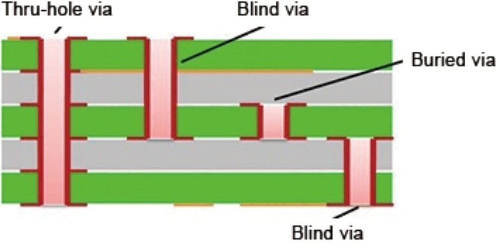
A blind via is a hole that connects two or more layers of a PCB without going through the entire board. Blind vias connect an internal layer to an external layer, stopping at the closest adjacent layer.
For example, in a 6-layer PCB, a blind via could connect layer 2 and layer 5 without penetrating all the way through layers 3, 4 and 6.
Diagram showing a blind via connecting two inner layers of a PCB [1]
Blind vias are fully plated and allow routing connections between internal layers without using up surface space. They help optimize routing density and shorten trace lengths.
Advantages of Blind Vias
Some key advantages of using blind vias:
- Save surface space – Since they do not go through the entire board, the via pads do not take up space on the outer layers. This leaves more room for component placement and routing on the surface.
- Improve routing density – By routing between layers with blind vias instead of on the surface, PCB routing channels can be optimized.
- Reduce layer jumps – A blind via provides a direct connection between two inner layers, eliminating the need to route a trace up and down through multiple layers.
- Cost effective – They require less drilling than a through hole via, reducing manufacturing costs.
- Allow for higher component density – With more routing done internally, components can be placed closer together on the surface.
Disadvantages of Blind Vias
Some disadvantages include:
- Limited connectivity – Since blind vias do not penetrate the full board, they can only connect the layers they span. Additional vias may be required to route signals to other layers.
- More difficult to manufacture – Creating the blind hole requires more complex drilling and costs more than drilling a straight through-hole.
- Not suitable for high-frequency or high-speed design – The stubs created can negatively impact signal integrity at high frequencies.
- Restrict component placement – Component pads cannot be placed over blind via holes, limiting placement options.
- Prone to failure – Due to the more complex manufacturing process, blind vias have a higher failure rate than standard through-hole vias.
When to Use Blind Vias
Blind vias work best for:
- High density, complex PCBs where routing channels are limited
- Multilayer boards where optimizing trace lengths is critical
- Low frequency digital and analog circuits where signal integrity is not impacted
They should be avoided in RF, microwave and other high frequency applications where maintaining signal integrity is a priority.
Blind vias provide flexibility in complex multilayer PCBs but require advanced manufacturing capabilities. They should be leveraged where design optimization is critical.
Via in Pad
What is a Via in Pad?
A via in pad refers to a plated through-hole via that is placed directly within the copper pad of a surface mount component. Instead of the via having its own discrete pad, it simply shares the pad of the component pin.
Via sharing pad with component pin [2]
The main purpose of a via in pad is to route signals from component pins on the surface layer to an internal layer. This optimizes routing by avoiding the need to use valuable surface traces.
Advantages of Via in Pad
Key benefits of using vias in pads:
- Save surface space – By routing internally from the component pad, no additional space is taken up by a discrete via pad.
- Reduce layer jumps – Direct connection from pad to inner layer reduces the number of layers a signal must cross.
- Improve signal integrity – The direct connection path minimizes parasitic inductance, resistance and capacitance.
- Simplify routing – With fewer traces needed on the surface layer, routing complexity is reduced.
- Lower costs – Reduces the number of drilled holes and amount of copper required.
Disadvantages of Via in Pad
Some downsides to consider:
- Limits component selection – Components must be chosen that can accommodate vias within pads without violating minimum spacing rules.
- Restricts pad size – The pad must be large enough for both the via and component pin.
- Reduces pad reliability – Drilling a hole in the pad can compromise solder joint integrity and increase risk of cracking.
- Creates tuning stubs – Can introduce impedance discontinuities that affect signal transmission, especially at high frequencies.
- Limits probe access – Probing component pins for debugging and testing becomes difficult with vias in pads.
- Requires advanced manufacturing – Laser drilling is typically required to accurately create small via in pad holes.
When to Use Via in Pad
Vias within pads work well when:
- Board space is extremely constrained.
- Optimizing high density component placement and routing.
- Layer transitions must be minimized for improved signal performance.
- Overall board layer count and drill hole count needs to be reduced for costs.
They should be avoided in RF circuits and other high frequency or high power applications where maintaining pad and connection reliability is critical.
Key Differences Between Blind Via and Via in Pad
| Parameter | Blind Via | Via in Pad |
|---|---|---|
| Definition | Connects two layers without fully penetrating PCB | Via placed within pad of surface mount component |
| Connectivity | Connects two adjacent layers | Connects surface layer to one or more inner layers |
| Pad on outer layers | No | Yes, shared with component pin |
| Manufacturing | Requires precise depth control when drilling | Requires precise laser drilling |
| Routing impact | Saves space on outer layers | Saves space on outer layers |
| Signal integrity | Can negatively impact high frequency signals | Direct connection minimizes parasitics |
| Cost | More expensive to manufacture | Reduces drilling costs |
| Reliability | Prone to failure due to process challenges | Can compromise pad and solder reliability |
Summary of Differences:
- Blind vias connect two adjacent inner layers, while via in pad connects surface layer to inner layer(s)
- Blind vias have no pad on outer layers but via in pad uses component pad
- Blind vias are more difficult to manufacture requiring depth control, via in pad uses laser drilling
- Both save routing space on outer layers but impact signal integrity differently
- Blind vias cost more but via in pad reduces drilling costs
- Blind vias have higher failure rate while via in pad can reduce pad reliability
The optimal via approach depends on PCB technology, design constraints, routing requirements and signal characteristics.
Frequently Asked Questions
What are some factors to consider when deciding between a blind via or via in pad?
Some key considerations include:
- Number of layers – Blind vias work better for complex multi-layer boards, via in pad simply needs 2+ layers
- High frequency signals? – Blind vias can cause reflections, via in pad has less impact on signal integrity
- Thermal relief requirements – Via in pad provides no thermal break, blind vias have discrete pads
- Routing constraints – If surface space is limited, vias in pad allow more optimization
- Manufacturing capabilities – Laser drilling is needed for reliable via in pad construction
- Component pin density – Vias in pad require adequate clearance between pins
- Testing access – Blind vias allow probing, via in pad limits access to component pins
Can vias cause reliability problems in PCBs?
Yes, both blind vias and vias in pads can create reliability risks if not designed and manufactured properly. Some common failure modes include:
- Pad cratering – Drilling through pad copper can fracture and weaken the pad
- Plating voids – Insufficient plating of via barrels can create open circuits
- Thermal cracking – Thermal cycles can propagate cracks from vias through solder and traces
- Moisture ingression – Plating voids can allow moisture penetration leading to corrosion
- Solder wicking – Solder can wick down into inadequately filled vias, depleting pads
What construction and material choices can improve via reliability?
Some best practices include:
- Laser drilled holes – More precise and cleaner drilling with less pad damage
- Thicker copper pads – Provides extra mechanical strength around via holes
- Plated through holes – Ensure via barrel is fully plated for conductivity
- Via in pad tenting – Polymer plug prevents solder wicking into via
- Solder masks defined pads – Prevent solder spreading from pad edges
- IPC Class 3 boards – Meet higher quality standards for holes and plating
What are some alternatives to using blind and via in pad vias?
Some alternatives include:
- Buried vias – Like blind vias but do not require an external connection
- Skip vias – Use multiple smaller stubs instead of one long via
- Staggered vias – Place vias in alternating pads minimizing stubs
- Microvias – Smaller vias with higher density routing
- Backdrilled vias – Only drill lower portion maintaining top pad integrity
How are impedance controlled vias designed?
Maintaining constant impedance through vias can be achieved by:
- Using via in pad to eliminate stubs
- Selecting via barrel size to match trace width for impedance
- Using ground vias surrounding signal via as return paths
- Adding annular rings around signal via pads on reference plane layers
- Filling unused area of drilled hole with epoxy to prevent resonance
- Using backdrilling and plugging to remove via stubs
Careful modeling and simulation of signals through vias is key to optimal impedance controlled design.
Conclusion
Blind vias and vias in pads provide methods to route signals between layers, optimizing density and performance in complex PCBs. Understanding the pros and cons of each approach allows designers to select the most appropriate via strategy.
Blind vias are best suited for high density multilayer boards where design flexibility is critical. Vias in pads optimize space and signal integrity when board real estate is extremely limited. With the right construction techniques, both via types can be highly reliable interconnect solutions.
Considering all the design, manufacturing and performance trade-offs is essential in leveraging these via technologies most effectively. This ensures the PCB platform provides the routing capabilities, signal fidelity and reliability required by the circuit and application.


Leave a Reply