Introduction
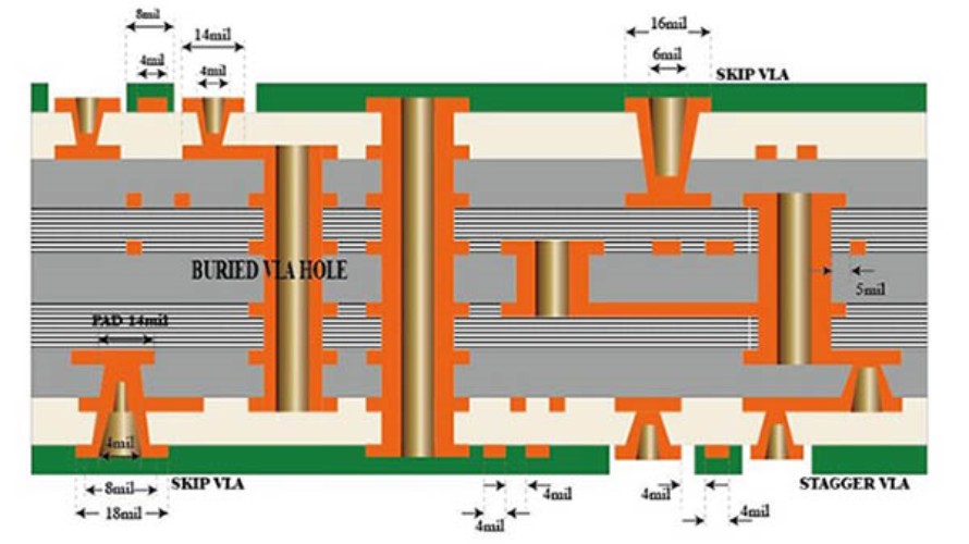
A via is a conductive hole that connects different layers of a printed circuit board (PCB). Vias allow signals to travel between layers. There are several types of vias:
- Through-hole vias – go through the entire PCB, connecting the top and bottom layers
- Buried vias – connect inner layers and are completely enclosed within the PCB
- Blind vias – connect an outer layer to one or more inner layers but do not go through the entire PCB
Blind vias are widely used in complex, multilayer PCBs as they offer several advantages over through-hole vias:
Key Advantages of Blind Vias
- Save space on outer layers – Allow more routing channels on outer layers since pads are only on connected inner layers
- Reduce drilling costs – Only drill down to the depth needed to connect required layers
- Improve signal integrity – Shorter path for signals reduces unwanted capacitance and inductance
- Enable high-density interconnections – Facilitate connections between components placed over vias on the outer layers
- Simplify routing – Provides flexibility for routing channels between inner layers under components
- Allow more layers – Using blind/buried vias enables designs with more PCB layers
This article will explore when and how to effectively utilize blind vias in your PCB design.
When to Use Blind Vias
Blind vias should be considered when:
- Connecting a component pad/pin to an inner layer but not to the opposite side of the board
- Routing high-speed signals between internal layers
- High component density is required on the surface of the PCB
- Additional routing channels are needed between internal layers
- Adding more PCB layers to facilitate complex routing
Some common situations where blind vias are beneficial:
1. Connecting pads on outer layers to inner planes
- Power or ground connections from surface mount pads to internal power/ground planes
- Reduce via stub length and loop inductance
2. Fanout from BGAs and other high density packages
- Facilitates routing from densely spaced ball grid array (BGA) pads
- Allows connections to internal layers without using space on outer layers
3. RF and high-speed signals
- Maintains signal integrity by providing a short path through reference planes
- Avoids creating stubs and unwanted capacitance of through-hole vias
4. Routing channels between inner layers
- Provides space for traces between inner layers under components
- Reduces congestion on outer layers
5. Multi-layer boards with high interconnect density
- Enable connections on boards with 8 layers or more
- Permits direct component attachment over buried vias
Blind Via Design Guidelines
To effectively implement blind vias, follow these design practices:
1. Plan blind via placement early
- Determine connections needed during schematic capture or layout planning
- Minimize use of through-hole vias to reduce drilling costs
2. Connect to appropriate pad/pin locations
- Choose pads that only connect to inner layers, not the entire board
- Avoid connecting blind vias to pads that must also connect to layers on the other side
3. Size blind vias appropriately
- Use larger diameters for high current connections
- Minimize size for high density routing areas
- Match drilling capabilities of your PCB manufacturer
4. Maintain spacing from board edges
- Keep blind vias away from board edges to avoid plating issues
- Maximum aspect ratio limits apply based on via depth
5. Provide sufficient annular rings
- Allow adequate annular ring width around pads for reliable connections
- Account for registration tolerances between layers
6. Limit use in thermal pads
- Avoid blind vias in large copper thermal pads where possible
- Can restrict heat flow if not filled properly
7. Fill blind vias
- Filling blind vias improves hole wall conductivity
- Consider thermal reliefs around filled vias in power planes
By applying these guidelines, you can successfully design blind vias that maximize connection density and simplify complex PCB routing.
Blind Via Fabrication and Testing
Specialized fabrication processes are required to produce blind vias during PCB manufacturing:
Laser Drilling
- Laser ablation used to selectively drill holes to required depths
- Excellent depth control and small diameter capability
- Limited by aspect ratio based on laser optics
Layer Alignment
- Requires precise registration between layers
- Achieved using fiducials markers visible on x-ray images
- Tight process controls needed to meet tolerances
Plating
- Electroless plating coats walls of blind vias
- Provides conductivity between layers
- Depth of plating can be challenging to control
Testing
- X-ray inspection confirms blind via structure
- Automated optical inspection (AOI) checks annular ring tolerances
- Continuity testing electrically verifies connections
- Impedance testing may be used for controlled impedance vias
Rigorous fabrication and inspection steps are implemented to produce reliable blind vias meeting the design requirements.
Comparing Blind, Buried and Through-Hole Vias
Blind vias have distinct advantages and disadvantages compared to buried and through-hole vias:<style> table { font-family: arial, sans-serif; border-collapse: collapse; width: 100%; } td, th { border: 1px solid #dddddd; text-align: left; padding: 8px; } tr:nth-child(even) { background-color: #dddddd; } </style> <table> <tr> <th>Via Type</th> <th>Advantages</th> <th>Disadvantages</th> </tr> <tr> <td>Blind Via</td> <td> <ul> <li>Save space on outer layers</li> <li>Limit drilling depth </li> <li>Simplify routing on inner layers</li> <li>Enable connections under components</li> </ul> </td> <td> <ul> <li>Require precise laser drilling</li> <li>Plating control can be difficult</li> <li>Limited aspect ratio</li> <li>Not suitable for pads connecting both sides</li> </ul> </td> </tr> <tr> <td>Buried Via</td> <td> <ul> <li>Interconnect inner layers only</li> <li>Avoid use of outer layer space</li> <li>Allow shortest routing between layers</li> </ul> </td> <td> <ul> <li>Challenging to inspect and rework</li> <li>Drilling alignment very critical</li> <li>Plating control is difficult</li> </ul> </td> </tr> <tr> <td>Through-Hole Via</td> <td> <ul> <li>Easy to fabricate and inspect</li> <li>No limit on aspect ratio</li> <li>Low cost process</li> <li>Connects all layers simply</li> </ul> </td> <td> <ul> <li>Uses outer layer space for pads</li> <li>Can cause signal integrity issues</li> <li>Not suitable for dense, multilayer boards</li> </ul> </td> </tr> </table>
Summary
- Blind vias connect outer layers to one or more inner layers without passing through the entire PCB
- Help increase routing density and simplify layout in complex multilayer boards
- Should be considered when routing signals between inner layers under components
- Provide a short path to power/ground planes reducing parasitic inductance
- Require advanced drilling and plating processes to fabricate reliably
- Offer an efficient interconnect solution complementing buried and through-hole vias
Used appropriately, blind vias enable optimized PCB designs meeting the increasing demands of modern electronics.
Frequently Asked Questions
Q1. What is the key advantage of using blind vias?
Blind vias’ main advantage is saving space on the outer layers of a PCB by allowing connections directly from the outer layers to desired inner layers without using through-hole vias. This facilitates complex routing in multilayer boards.
Q2. What fabrication process is used to create blind vias?
Blind vias are fabricated using laser drilling. A laser is used to selectively ablate the material only to the depth required to connect the layers needed. The laser can precisely drill to a specific depth.
Q3. How can you determine if blind vias are required in a design?
Analyze the interlayer connectivity requirements during layout planning. Blind vias should be considered if signals or pads need to connect to inner layers without passing through to the other side, especially under high density components.
Q4. What special design practices should be followed when using blind vias?
Use large annular rings, pay attention to aspect ratio limits, follow minimum spacing rules, and plan early to minimize use of through-hole vias. Appropriate blind via placement and sizing is key.
Q5. Can buried and blind vias be used in the same PCB?
Yes, buried and blind vias can complement each other in a design. Buried vias interconnect two or more inner layers only. Blind vias connect outer layers to one or more inner layers. Using both provides routing flexibility.


Leave a Reply