Introduction
Printed circuit boards (PCBs) and high-density interconnect (HDI) PCBs are key components in modern electronics. They provide the foundation for mounting and connecting electronic components. While they share some similarities, there are important differences between traditional PCBs and HDI PCBs related to their design, manufacturing, and use. This article will compare and contrast PCB and HDI technologies and provide guidance on when to use each approach.
PCB Basics
A printed circuit board is a flat surface made of insulating material used to mount and connect electronic components using conductive tracks and pads. The board itself is non-conductive, usually made of laminated layers of fiberglass or other composite materials. Copper foil conductive traces are patterned on the board to provide electrical connections between components.
PCBs provide both the structural foundation and the wiring between electronic components. They are ubiquitous in all types of electronic devices and equipment. The key elements of a PCB include:
- Substrate – The flat, insulating board material. The most common material used today is FR-4 fiberglass.
- Conductive layers – Layers of copper foil that are etched to form the conductive traces and pads.
- Holes/vias – Holes that are drilled or punched in the board to allow connections between layers. These are plated with copper to become conductive vias.
- Solder mask – Coating that is selectively applied over the substrate and copper layers. It protects copper traces from shorting and oxidation.
- Silkscreen – Printing applied to the solder mask to indicate component locations, labels, logos, etc.
- Finish – Plating applied to exposed copper pads and vias to facilitate soldering. Common finishes are HASL, ENIG, and immersion silver.
PCB Layout and Design
The specific layout of a PCB depends on the circuit design and electronic components used. PCB layout involves positioning and routing copper tracks to make the required connections between components. Multi-layer boards will also require designing power and ground planes within the board layers.
Key PCB design considerations include:
- Component placement – Optimizing component positions to minimize track lengths andcrosstalk. High-speed and high-frequency components require particularly careful placement.
- Routing – Tracking routing to ensure clean routing with appropriate spacing and isolation between traces.
- Signal integrity – Managing impedance, cross-talk, electromagnetic interference (EMI), and other signal integrity issues.
- Thermal design – Ensuring adequate thermal management through board layout. This includes providing sufficient copper ground planes and thermal vias.
- Manufacturability – Designing the board so it can be fabricated with standard PCB processes.
PCB Fabrication and Materials
PCBs are fabricated by bonding copper foil onto substrate materials, usually fiberglass composites. The foil is then selectively etched away to form the desired circuit patterns.
Some key points regarding traditional PCB fabrication:
- Multiple layers are bonded together using adhesive sheets called prepreg. Completed boards usually have between 2 and 12 conductive layers separated by insulating prepreg.
- Holes are drilled through the board and plated with copper to form conductive vias between layers.
- Minimum trace/space is typically around 6 mil (0.15mm) when using standard fabrication processes.
- FR-4 glass reinforced epoxy is the most common substrate material used. It provides good Physical and electrical properties at low cost.
- Copper thicknesses generally range from 1⁄2 oz (18 μm) to 2 oz (70 μm) per layer. Heavier copper layers improve conductivity and current carrying capacity.
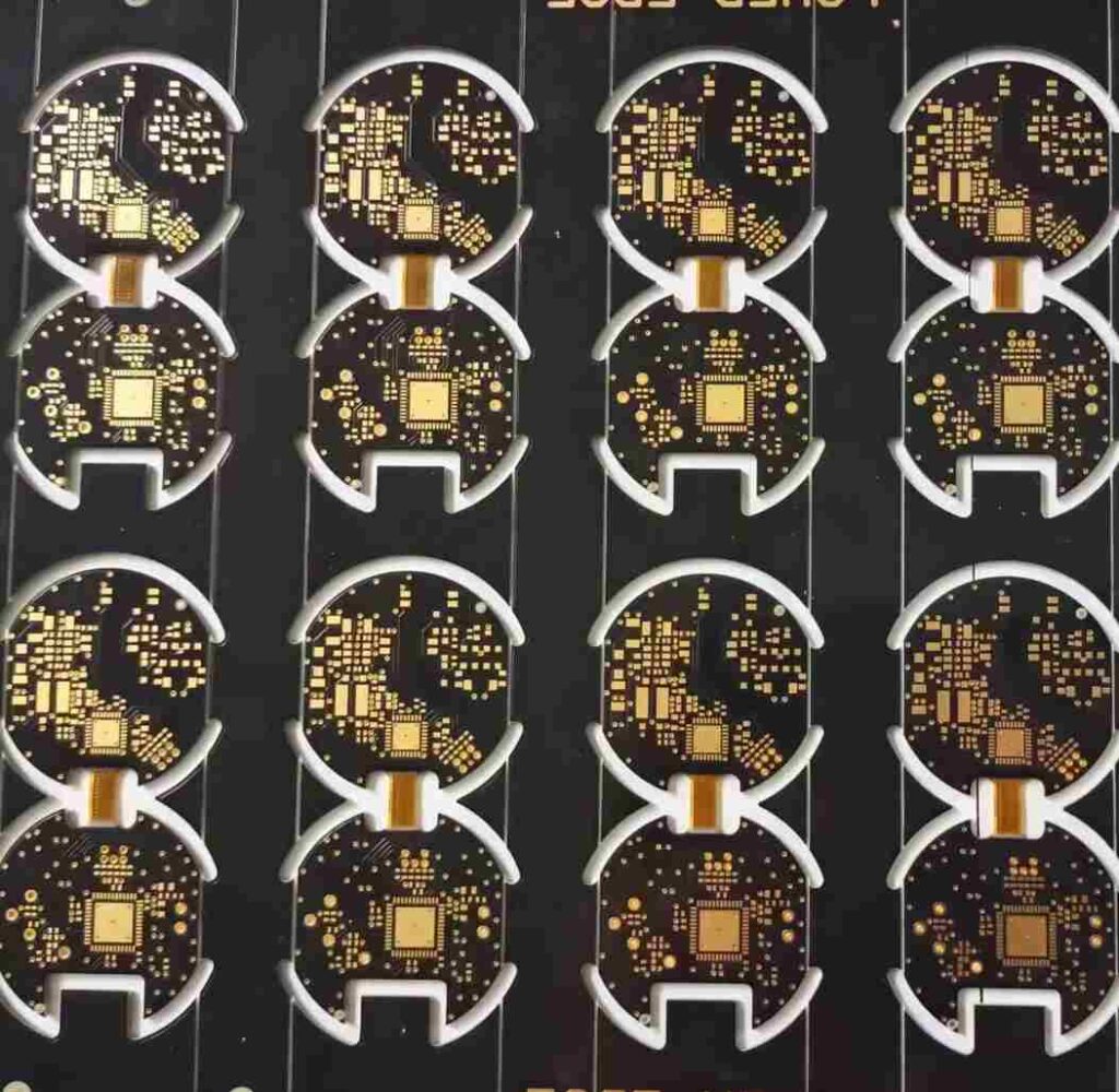
HDI PCB Overview

HDI (High Density Interconnect) PCBs were developed to support increasing interconnect density requirements driven by high pin count components and shrinking product sizes. They allow much higher trace densities compared to standard PCBs.
Some key characteristics of HDI PCBs:
- Trace/space can be under 3 mils (0.075mm), sometimes below 1 mil for microvia HDI. This supports high I/O components with pin pitches under 100 microns.
- HDI utilizes thinner dielectric materials which have lower glass transition temperatures. This enables finer lines/spaces because the materials can withstand higher lamination pressures.
- Blind and buried vias are used extensively for layer-to-layer interconnections rather than through-hole vias. This simplifies routing dense designs.
- Thin core boards or coreless constructions are often used, reducing layer thickness. Overall board thickness can be under 62 mils (1.5mm).
- Fine line circuitry is combined with high-density chip packaging like BGA, CSP, and flip chip devices. These have pin densities up to about 1500 pins per square inch.
In summary, HDI allows much higher wiring densities to support increased component packaging densities and interconnect requirements. The tradeoffs include more complex fabrication and potentially higher costs.
HDI Design and Materials
Implementing a design using HDI technology requires some different design considerations compared to standard PCBs:
Board Materials
- Thin dielectric materials are used as insulators between layers. Common materials include polyimide, liquid crystal polymer (LCP), and others with low glass transition temperatures.
- Dielectrics are as thin as 2 mils for coreless constructions. This allows very tight trace spacing.
- Cores are typically thin materials like bismaleimide triazine (BT). Overall board thickness can be under 62mils.
Trace Routing
- Traces can be under 1 mil line width and space. Typical minimums are around 2-3 mils.
- Vias are generally blind or buried rather than through-hole vias. This avoids the need to drill through the entire board.
- Laser drilling can produce microvias down to 6-10 mils diameter for interlayer connections.
- Stacked microvias are often used when even higher connection densities are required.
Layer Stackup
- A typical HDI stackup has 4-8 conductive layers separated by thin dielectrics.
- There may be several groups of fine line layers separated by thin cores or coreless constructions.
- Both fine line and conventional traces can be designed on different layers as needed.
- High-speed signals are routed on controlled impedance dielectric layers.
Board Fabrication
HDI boards require specialized fabrication processes capable of producing extremely fine features:
- Laser drilling forms blind and buried vias. Mechanical drilling achieves 6-8 mil vias.
- Thin materials with low glass transition temperatures are laminated under high pressure and temperature to bond layers.
- Plasma processes can selectively etch extremely fine circuit patterns under 1 mil line/space.
- Thin copper foils down to 1⁄3 oz (9 μm) are used along with subtractive etching to produce fine traces.
- Sequential lamination combines conventional PCB and fine line HDI processes on a single board.
Cost Implications
The specialized materials, fabrication processes, and design complexity of HDI results in higher costs:
- Base material costs are higher for the thin dielectric layers, thin cores, and fine copper foils.
- HDI fabrication has lower yields and throughput compared to conventional PCBs.
- There are additional process steps associated with laser drilling, plasma etching, and thin core/coreless lamination.
- HDI design is more complex and time-consuming due to blind/buried vias, dense routing, and impedance control.
Therefore, HDI implementation involves a cost versus benefit tradeoff for increased performance.
Comparison of PCB and HDI
Here is a summary comparison between standard PCBs and HDI technology:
| Parameter | Standard PCB | HDI PCB |
|---|---|---|
| Substrate Materials | FR-4 glass epoxy | Polyimide, BT, LCP |
| Dielectric Thickness | 2-4 mils typically | 2 mils or less |
| Conductor Thickness | 1⁄2 oz (18 μm) typical | 1⁄3 oz (9 μm) or less |
| Trace Width/Space | 6 mil (0.15mm) typical | 2-3 mil (0.05-0.075mm) typical |
| Via Type | Through-hole and blind vias | Blind/buried microvias |
| Via Size | 8-12 mil diameter typical | 6-10 mil microvias |
| Layer Count | 4-16 layers typical | 4-12 layers typical |
| Board Thickness | 62 mils (1.5mm) typical | As low as 25 mils (0.6mm) |
| Fabrication Process | Standard PCB processes | Additional HDI processes |
| Cost | Lower | Higher due to advanced materials and processes |
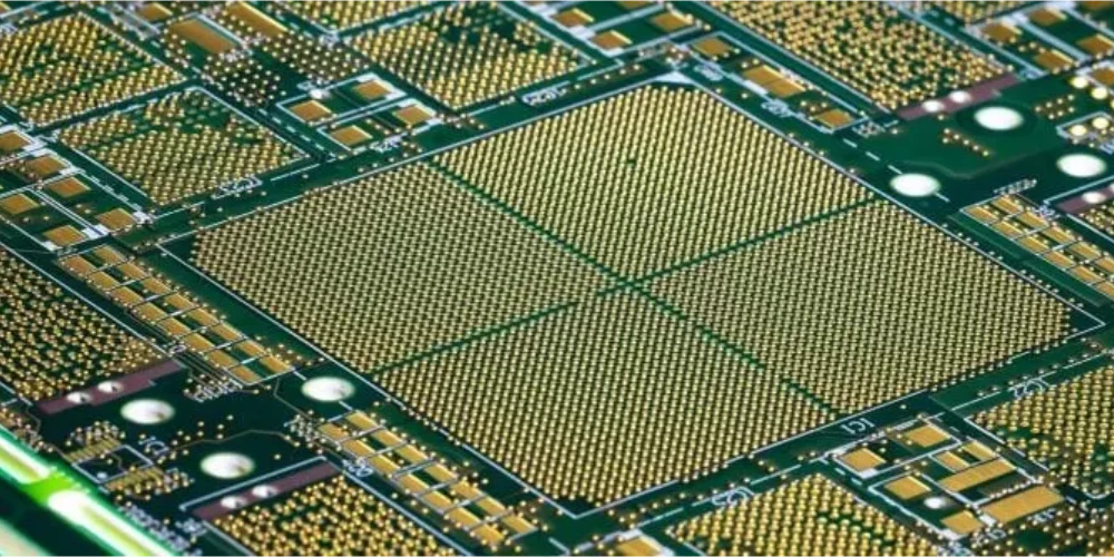
Figure 1 below visually compares the difference in trace densities between standard PCB and HDI boards:
Figure 1. Comparison of trace densities on standard PCB (left) versus HDI PCB (right). Image source: ResearchGate
When to Use PCB vs HDI
Here are some guidelines around when to implement a design with standard PCB technology versus when HDI should be utilized:
Use standard PCB technology when:
- Design has low-mid pin count components with pin pitch above 0.5mm.
- Only a few layers (4-8) are required to route design.
- Thickness constraints allow 62 mil or thicker board.
- Electrical performance requirements are easily achieved with FR-4 dielectric.
- Overall lowest cost is the primary objective.
Utilize HDI technology when:
- Design uses high pin count components with pin pitch below 0.5mm.
- Large number of layers (8+) would be needed for routing with standard processes.
- Thickness close to 1mm or less is required.
- Maximum performance is needed to meet timing, impedance, or signal speed requirements.
- High product miniaturization is needed.
In summary, HDI should be strongly considered when the interconnect density necessitates trace widths and spaces below 4 mils, and/or when overall board thickness under 62 mils is required. The advanced HDI materials and processes enable meeting these requirements at a higher manufacturing cost.
HDI allows supporting cutting edge electronic package and interconnect requirements driven by products like smartphones, tablets, IoT devices, and other compact electronics. The tradeoff is that HDI PCB fabrication has lower throughput and yields versus standard PCBs, resulting in higher costs.
Frequently Asked Questions
What are some key differences between HDI and standard PCBs?
Some key differences are:
- HDI utilizes thinner dielectric materials allowing tighter trace spacings below 3 mils.
- HDI has minimum trace widths around 2 mils versus 6 mils for standard PCBs.
- HDI incorporates blind and buried microvias while standard PCBs utilize through-hole vias.
- HDI boards can be less than 25 mils thick while standard PCBs are typically 62 mils or thicker.
- HDI fabrication requires specialized processes like laser drilling, plasma etching, and high pressure lamination.
Why does HDI allow higher component packaging densities?
The combination of thin dielectrics, fine line traces, and buried microvias enables routing the very tightly spaced pads of high I/O components. This lets HDI support high density component packages, such as fine pitch BGAs, CSPs, and flip chips.
What are microvias?
Microvias are very small vias with diameters typically between 5-10 mils that are used to interconnect layers on HDI boards. They are formed by laser drilling and allow connections without using through-hole vias. Stacking offset microvias enables even higher connection densities.
Does HDI replace the need for standard PCB technology?
No, HDI complements rather than replaces standard PCB technology. Many designs will utilize both HDI and conventional PCB fabrication processes as needed for routing and meeting thickness and density requirements across different board regions.
Are there any disadvantages to using HDI?
Yes, the main disadvantages are increased complexity for both HDI design and manufacturing. Developing an HDI design requires specialized expertise, and HDI fabrication involves lower yields along with more process steps that ultimately increase costs.


Leave a Reply