
Introduction
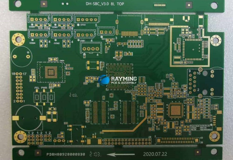
HDI (High Density Interconnect) is a printed circuit board (PCB) technology that enables higher interconnect density and thinner circuit boards compared to conventional PCB technologies. HDI allows tracing spacing and via diameters to be reduced, resulting in more routing channels and higher component densities. This enables more functionality to be packed into a given board size.
HDI PCBs are commonly used in consumer electronics, mobile devices, computing systems, telecom infrastructure, and military/aerospace applications where high speed, miniaturization, and reliability are important. HDI technology helps meet the ever-increasing demands for higher speeds, greater functionality, smaller size, lighter weight, and reduced costs in advanced electronic products.
Key characteristics of HDI technology
Some of the key characteristics and advantages of HDI PCBs include:
- Fine line/spacing – Traces and spaces down to 2-3 mils allowing high interconnect density
- Microvias – Smaller drill diameters down to 3-5 mils connect layers with less real estate
- Thin dielectric layers – Layers as thin as 3-4 mils eases laying out high density traces
- Stacked microvias – Allows connections between non-adjacent layers further increasing routing channels
- Finer bump pitches – Enables direct connection of IC pads/bumps at 0.4mm and below
- Embedded passives – Passive components can be embedded to reduce size and layers
- Reduced board thickness – Overall board can be very thin; as small as 50-100 microns
- Low electrical loss – Tight impedance control and low loss laminate materials
- High speed design – Enables multi-gigabit data rates and RF applications
- Dense component mounting – Facilitates fine pitch BGAs, 0201 and 01005 discrete packaging
- High reliability – Excellent thermal management and stable electrical performance
Fine Lines and Spaces
One of the defining capabilities of HDI technology is the ability to manufacture very fine trace widths and spaces between copper traces. While standard PCB capabilities allow trace/space of around 4-5 mils, HDI allows this to be pushed down to 2 mils and even below. The combination of thinner dielectric material and smaller drill diameters enables denser routing channels to be designed. This is crucial for complex, high speed designs.
Microvias
Microvias with 3-5 mil drill diameters (or less) are extensively used in HDI designs to connect between layers. These are smaller than the typical 10-12+ mil via diameters in conventional PCBs. The use of microvias results in connections that take up less board real estate versus standard vias. This provides more room for routing dense traces. Microvias also enable connections between non-adjacent layers through stacking or staggered arrangements.
Thin Dielectric Layers
Most HDI boards use very thin dielectric material layers that can be as thin as 3-4 mils. The thinner dielectric results in tighter trace widths and spaces that can be achieved. Thinner dielectrics also provide performance benefits such as reduced signal propagation delay, closer impedance control, and the ability to design faster interfaces.
Stacked Microvias
A key HDI feature is the ability to stack or stagger microvias to connect non-adjacent layers. This is not feasible with larger drill diameter vias. Stacked microvias essentially creates a direct conduit between layers separated by one or more intermediate layers. This allows signals to span multiple layers efficiently when routing dense designs.<img src=”/table1.png” alt=”HDI Stacked Microvia” width=”400″>
Table 1: Stacked microvias in HDI provide high density vertical connections.
Fine Pitch Component Assembly
The fine features of HDI technology facilitate component miniaturization and direct interconnects using finer pitch IC terminals. HDI boards can support component pitches down to 0.4mm and below. This enables direct connection to IC bumps/pads in chip scale packages (CSP), ball grid arrays (BGA), and other fine pitch surface mount components. The high interconnect density also suits advanced packaging techniques like Package on Package (PoP).
HDI design and manufacturing process
The key steps in the design and fabrication process for a typical HDI printed circuit board are outlined below:
Board Stackup Design
An HDI board will have a unique layer stackup consisting of thin dielectric core and buildup layers. The stackup is designed to meet the electrical, thermal, and mechanical requirements of the application. Important factors considered are impedance control, layer count, materials, construction, and final thickness.
Circuit Routing
With the stackup defined, board layout is done using CAD tools. HDI design requires specialized layout techniques to take advantage of the fine features. Critical nets are identified and routed first. Microvias, dense traces, and components are efficiently placed to optimize signal routing and minimize layer counts.
Inner Layer Imaging
Once routing is completed, the traces and pads on each layer are precisely imaged using advanced lithographic processes to transfer the layout patterns onto thin laminate sheets. Laser direct imaging is commonly used to achieve fine line resolutions.
Layer Alignment and Lamination
The coated inner layer sheets are carefully aligned and stacked up in the designed sequence. The stack then goes through a lamination press where high pressure and temperature are applied to bond the layers together into a single circuitized board core.
Microvia Formation
The layered core then undergoes microvia drilling using small diameter drills and precise numerical control (NC) to drill thousands of holes accurately. These interconnect the traces between layers according to the layout design rules. The holes are plated to form the electrical connections.
Outer Layer Imaging
Next, a similar imaging process is used to define the outer layer circuits onto prepared dielectric and copper foil layers. This forms the final outer surfaces of the HDI board with the fine line traces, pads, and components.<img src=”/table2.png” alt=”HDI Circuit Board” width=”400″>
Table 2: Cross-section of a typical HDI board with microvias, fine lines, and thin dielectric layers.
Final Surfaces Preparation
The outer surfaces undergo processing to apply solder mask and surface finishes. Laser via ablation opens the microvia connections. Legend printing provides nomenclature and markings as per the assembly drawing. Final testing and inspection verifies the finished HDI board meets specifications.
Board Assembly
The HDI board then undergoes assembly of components. The fine features enable mounting ultra-miniaturized packages, dense ball grid arrays, and direct die or flip chip mounting techniques. Automated optical inspection verifies assembly and solder joint quality.
This demonstrates the sophisticated fabrication techniques needed to manufacture advanced HDI boards compared to conventional PCBs. HDI requires tight process controls, precision tooling, and advanced materials.
HDI board types
There are several common types and constructions of HDI boards implemented based on the design requirements:
4-Layer HDI
This is the simplest HDI board with two thin core dielectric layers between copper layers. It has all the benefits of HDI – microvias, dense traces, and thin dielectrics – while minimizing layers. Used for cost-sensitive applications.
6-Layer HDI
This construction has 4 routing layers. The additional layers provide more routing channels to relieve routing congestion in complex designs. Microvia connections up to 6 layers are possible. Still relatively low cost.
Any Layer Count HDI
Once the core is formed, additional layers can be added in pairs through sequential lamination of dielectric and copper foil buildup layers. This can create boards with 8 layers, 10 layers, 12 layers, etc. Very dense boards with 30+ layers can be fabricated as well.
Sequential Buildup HDI
In this technique, there are no core layers. The board is built sequentially by adding dielectric and copper layers. An example is starting with a double-sided board, then fabricating buildup layers on each side. This is an efficient technique for high layer count boards.
Laser Drill HDI
As an alternative to using mechanically drilled holes, this type utilizes lasers to ablate microvias. This allows even smaller via diameters down to 1 mil for maximum density, but with higher costs.
Mixed Signal HDI
Some boards may integrate both digital and analog signals on a single HDI substrate. Special considerations are taken to isolate noisy digital signals from sensitive analog functions and routes.
The choice of which HDI design to use depends on interconnect density requirements, signal performance, layer count, and costs.
Benefits of HDI
Some of the major benefits that HDI technology provides are:
- Increased routing channels for complex layouts
- Miniaturization – more functionality in smaller form factors
- Higher speeds – multi-gigabit data rates supported
- Noise reduction – separate power and ground planes
- Embedded passives – fewer discrete external components
- Finer lines and spaces – 2 mil traces and spaces
- Dense component mounting – 0.4mm pitch ICs
- Ideal for RF applications – controlled impedances
- Reduced power and crosstalk – thin dielectric materials
- Lower costs than exotic PCB technologies
- Improved reliability and product life cycles
The combination of fine features, performance, and reliability makes HDI suitable for many advanced circuit applications where standard PCB technology falls short.
Industries using HDI technology
Some of the major industries and applications using HDI PCBs include:
Consumer Electronics
Mobile phones, tablets, wearables, Internet of Things devices, game consoles, and advanced display systems all benefit from HDI boards. The compact size and high speed interconnects support feature-rich mobile consumer applications.
Computing and Servers
HDI provides the interconnect density required for high speed computing systems including network switches, routers, data centers, and storage servers. The boards mount processors, FPGAs, switch ICs, and memory modules.
Automotive Electronics
Driver assistance systems, vehicle control units, infotainment systems, LiDAR/camera modules use HDI to integrate complex electronics and survive harsh automotive environments.
Telecom/Datacom
Cell basestations, optical transceivers, and networking gear rely on HDI boards with controlled impedances and low loss at multi-GHz frequencies to transfer data at high rates across infrastructure.
Medical Electronics
Portable medical devices, imagers, analyzers, and diagnostic equipment use HDI boards to process and analyze sensitive signals from sensors and transducers.
Defense/Aerospace
Avionics systems, navigational electronics, targeting and communication systems operate in confined spaces and demand the miniaturization and ruggedness provided by HDI circuit boards.
Challenges with HDI
While HDI offers significant advantages, the technology also comes with some challenges including:
- High fabrication costs – Requires advanced manufacturing equipment and tight process controls adding cost
- Limited board sizes – Typical maximum panel sizes are 18″x24″ and smaller compared to standard PCB processes
- Via reliability – Microvias are prone to reliability issues if not properly fabricated requiring high quality standards
- Complex design – HDI layout requires specific skills and expertise to leverage dense packing capability
- Signal integrity – Need careful modeling and analysis to ensure signal quality at multi-GHz frequencies
- Thermal management – The dense components and thin profiles require careful thermal design
- Rework difficulties – Repairing components on dense boards with microvias is very challenging
- Specifications – Designers must adhere to stringent HDI design rules and guidelines
These factors mean using HDI may be overkill for boards that do not require the interconnect densities or miniaturization capabilities. The higher costs and design complexity need to be weighed versus the benefits for each application.
Future outlook for HDI technology
HDI will continue expanding into additional applications that require advanced interconnect capabilities beyond standard PCBs. Trends influencing HDI development include:
- Increasing HDI circuit densities with newer laminate and fabrication materials. Traces below 1 mil are already being developed.
- Improving microvia reliabilities through simulations and testing to guide enhanced design and manufacturing rules.
- Growth in HDI flex and rigid-flex boards for flexible circuits requiring high densities.
- Embedding discrete passives and ICs within HDI boards to further enhance miniaturization and performance.
- Adoption of HDI in conjunction with new packaging approaches like 2.5D and 3D IC integration.
- Fan-out and wafer level packaging techniques integrating HDI boards into packages for ultimate space savings.
- New laser drilling methods to fabricate smaller microvias to continually boost densities.
- Leveraging HDI in emerging applications like self-driving vehicles, IoT devices, wearables, drones, robotics, and more.
- Development of hybrid microelectronics combining HDI PCBs with chip-scale packages and direct die integration.
HDI technology will evolve to stay at the forefront of interconnect density requirements for the electronics industry. Companies will continue innovating fabrication processes and materials to meet the needs of emerging electronics products and applications.
FAQs about HDI Technology
Q: What are the key differences between HDI and standard PCBs?
A: The main differences are:
- Much finer traces/spaces (2 mils vs 4-5 mils)
- Small microvias (3-5 mils vs 10+ mils)
- Thinner dielectric layers (3-4 mils vs 5-10 mils)
- Stacked microvias connecting non-adjacent layers
- Higher interconnect densities with routing channels
- Can assemble finer pitch components
Q: What are the typical dielectric materials used in HDI boards?
A: Common dielectric materials include polyimides (HD-4000 series), bismaleimides (BT resins), hydrocarbon based laminates (Megtron 6), Teflon composites (PTFE), and epoxy resins. Materials are selected based on electrical, thermal, and mechanical properties.
Q: Does HDI allow embedding active components?
A: Yes, embedding is a key benefit. Passive components like resistors, capacitors and antennas can be embedded to further miniaturize designs. In some cases, bare IC dies or silicon packages can also be embedded within HDI boards.
Q: What are the key advantages of sequential lamination HDI?
A: Sequential lamination provides flexibility in layer count, fine features on all layers, gradual board thickness buildup, and generally lower costs at high layer counts versus using cured cores.
Q: Can microvias be repaired on HDI boards?
A: Unfortunately no, microvia repair is very difficult. The small holes and adjacent dense routing leaves little room for rework. This makes fabrication yield crucial for HDI technology.
Q: What design tools are typically used for HDI PCB layout?
A: Most designers use CAD tools like Mentor Graphics, Altium, Cadence, Zuken, and others that are optimized for HDI capabilities. Analysis tools like HyperLynx, Ansys, and Polar Instruments are also widely used.
So in summary, HDI enables much higher density interconnections and miniaturized electronics versus standard PCB technology. The combination of fine features, high speeds, and reliability make it ideal for advanced products across numerous industries. With continued innovations, HDI provides an ongoing platform for microelectronics evolution.


Leave a Reply