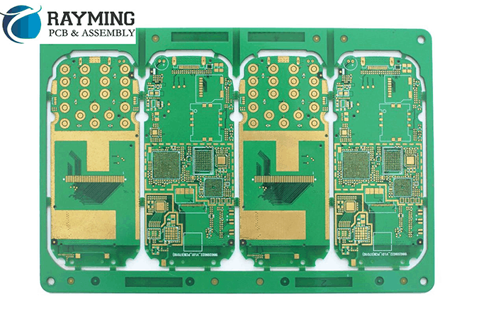
HDI (High Density Interconnect) PCBs are printed circuit boards with a higher wiring density than conventional PCBs. They allow integrated circuits to be packed more densely on a PCB and enable smaller components, traces and spaces. This allows for design miniaturization and increased functionality.
However, HDI PCBs also have some disadvantages compared to conventional PCBs:
Higher Cost
The foremost disadvantage of HDI PCBs is their higher fabrication cost compared to conventional PCBs. This is due to:
Smaller Traces and Spaces
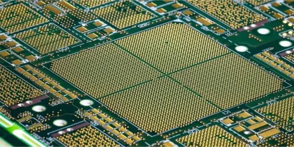
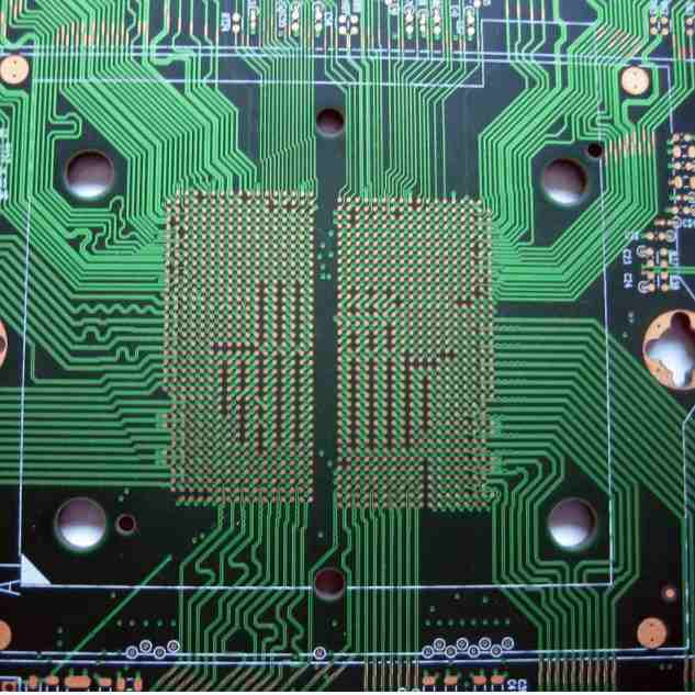
HDI PCBs have much finer lines and spaces. A conventional PCB will have minimum trace widths and spaces of around 6-8 mil while HDI PCBs can go down to 2-3 mil. This requires more accurate manufacturing equipment.
More Layers
HDI PCBs usually have 6 to 12 layers or more. Standard PCBs typically have only 2 to 4 layers. More layers increases material costs.
Tighter Tolerances
The tighter traces, spaces and via diameters require each PCB layer to be aligned more accurately. This demands better registration control during fabrication.
Additional Processing Steps
Extra steps like laser drilling for microvias and sequential lamination with accurate alignment for the buildup layers increases fabrication time and cost.
Lower Yields
The dense packing and tiny features on HDI PCBs provide less margin for error. A small defect can cause electrical shorts or opens, lowering manufacturing yields. This further adds to cost.
Lower Reliability
With high density routing, HDI PCBs are more susceptible to problems like:
- Delamination – Separation of buildup layers due to thermal stresses.
- Thermal issues – Dense packing leads to localized heating which can cause reliability problems.
- EMI/EMC – Closely spaced traces can cause more interference.
- Popcorning – Trapped moisture in the PCB laminates can vaporize during reflow soldering and cause surface blisters or delamination.
Complex Design
The complex stackup and high density routing requires designers experienced in HDI techniques. Extensive analysis and simulation of the electrical, thermal and mechanical aspects is needed.
Longer Development Time
The specialized design complexity along with fabrication and assembly process development results in a longer time to market compared to standard PCBs.
Challenging Rework and Repair
The fine features make manual rework and field repair of HDI PCB assemblies very difficult. Specialized equipment may be required.
Limited Suppliers
As HDI PCB fabrication requires advanced processes and equipment, there are fewer suppliers capable of manufacturing them, especially at lower volumes.
Fabrication Process Limitations
There are some limitations in terms of minimum trace widths, microvia sizes and capture pad sizes based on the fabrication processes available.
Laser Drilled Microvias
Laser drilling can reliably drill microvia holes down to around 25-50μm. Below this, high density plasma etching must be used which has lower throughput.
Line Width/Space
Line widths below 2 mils require semi-additive plating processes. Sub-micron traces need expensive lithographic processes.
Capture Pad Size
The capture pad size around a microvia is dictated by theAccuracy of the laser drill. Smaller pads increaseopens risk. Minimum pad sizes are around 4-5 mils.
Impact on PCB Performance
The increased wiring density and smaller features have pros and cons in terms of electrical, thermal and mechanical performance:
Electrical Performance
| Parameter | Effect |
|---|---|
| Signal Speed | Faster signal propagation due to thinner dielectric layers |
| Crosstalk | Worse due to tighter trace spacing |
| EMI/EMC | More interference due to high frequency signals in proximity |
| Impedance Control | Tighter impedance tolerances are possible |
| Signal Integrity | Improved with precise control of trace dimensions and material properties |
Thermal Performance
| Parameter | Effect |
|---|---|
| Heat Density | Increased due to dense component packing |
| Thermal conductivity | Improved through-hole plating helps dissipate heat |
| Reliability | Localized heating and hotspots can reduce long term reliability |
| Warpage | Can worsen due to mismatch in coefficients of thermal expansion between buildup layers |
Mechanical Performance
| Parameter | Effect |
|---|---|
| Stiffness | Can reduce with more layers and thin dielectrics |
| Dudile/Flexural Strength | Depends on materials used in the stackup |
| Vibration/Shock Resistance | Degrades with more layers |
| Resistance to CTE Mismatch | Poorer due to more interfaces prone to delamination |
| Environmental Resistance | Moisture absorption and related failures increase |
Applications Best Suited for HDI PCBs
Despite the higher cost and limitations, HDI PCB technology provides the interconnect density needed in many advanced electronics products. Some applications that are ideal candidates for HDI PCBs are:
- Smartphones – To integrate advanced components like application processors, modems, memory and sensors in a compact form factor.
- Wearable devices – Miniaturization and flexibility requirements make HDI suitable.
- Internet of things devices – For fitting more functionality into small footprints.
- Medical devices – Where reliability, signal integrity and space constraints are critical.
- Automotive electronics – High density interconnection and vibration resistance needed.
- Aerospace/military – Size and weight reduction critical despite lower volume requirements.
- Servers/data centers – High speed signaling and thermal management provided by HDI PCBs.
HDI PCBs provide the best performance versus size tradeoff for advanced portable consumer products. Their higher cost can be justified for mission-critical devices where reliability and electrical performance are paramount. Lower volume applications in automotive, aerospace and medical leverage HDI where standard PCB technology falls short.
HDI PCB Manufacturing Techniques
There are a few key advanced manufacturing processes that enable the high wiring density and stacked layer structure of HDI PCBs:
Buildup Dielectric Layers
The core layers are fabricated using standard lamination. Additional thinner dielectric layers are added sequentially over the core using buildup processes. Common techniques include:
- Photoimageable Dielectrics – Dry film or liquid photopolymers that are photolithographically patterned and cured.
- Plasma Polymerization – Layers deposited from gas precursors using plasma enhanced chemical vapor deposition.
- Sputtered Films – Dielectric films like SiO2 deposited using sputter deposition.
Microvias
Blind and buried vias with diameters below 0.15mm are drilled using lasers. UV lasers like Nd:YAG Quadrupole Resonance (QR) can drill 25-50μm microvias. CO2 lasers drill larger 85-150 μm vias.
Fine Line Patterning
To form dense multi-layer interconnects, the dielectric layers are metallized using:
- Subtractive Processes – Full copper patterning using lithography and etching.
- Semi-Additive Processes – Electroless metal deposition followed by lithographic patterning.
- Modified Semi-Additive Processes – Combines electroless and electrolytic plating for thicker and denser traces.
Stackup Alignment
Laser drilled fiducials on each layer provide alignment accuracy between layers of around 25-50μm for stacking HDI layers. Tighter alignment yields better routing density.
Trends in HDI PCB Technology
HDI PCBs have seen steady increases in density and layer count driven by electronics miniaturization trends. Some key trends shaping their evolution are:
- Finer Routing Features – Line widths and spaces below 2 mils and microvias smaller than 25μm are becoming mainstream. This allows greater routing density.
- Higher Layer Counts – HDI designs with 16-24 layers allow increased wiring capacity and more routing channels. High density interconnect in 3 dimensions.
- Embedded Passives – To save space, passive components are fabricated within the HDI layers. Examples are embedded resistors and capacitors.
- Any Layer Microvias – Microvias can penetrate anywhere across the stackup, not just adjacent layers. This simplifies routing congestion.
- Blind and Buried Microvias – Allow connections between inner layers without using through holes. Further increases routing density.
- Laser Drilled Trenches – Replaces conventional routing with laser etched trenches in the dielectric. Saves space compared to patterned copper traces.
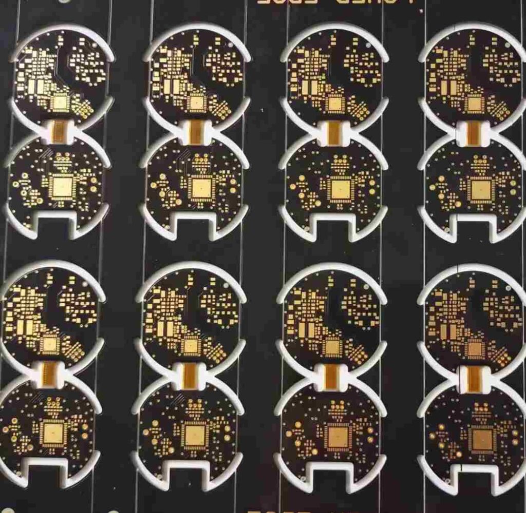
- Flexible and Rigid-Flex HDI – Implements HDI stackups using flexible polyimide dielectric materials. Enables flexible PCB sections.
- Heterogeneous Integration – Combining HDI, embedded passives, flexible and rigid PCB sections for highly integrated Systems-On-Package (SOP) solutions.
HDI PCB Design Guidelines
To leverage the full capability of HDI PCB technology and avoid pitfalls, designers should follow certain guidelines:
Stackup Planning
- Minimize the number of layers. Optimize routing to avoid exceeding 16 layers if possible.
- Use thinner dielectrics for faster speeds but ensure reliability and manufacturability.
- Place ground planes adjacent to signal layers to enhance signal integrity.
- Watch glass transition temperatures (Tg) when combining materials.
Layout Considerations
- Follow manufacturer design rules for trace widths, spacing, microvias, capture pads etc.
- Use grids appropriate for features. Such as 0.5mil grid for under 4mil lines/spaces.
- Avoid 90° traces changing layers. Use 45° or wider angles.
- Design balanced differential pairs with same overall length and proper spacing.
Thermal Management
- Ensure copper balances to avoid thermal gradients causing warp/twist.
- Watch for thermal spots near heat generating components like BGAs. Use thermal vias if needed.
- Include large copper fills on unused areas for heat spreading.
Signal and Power Integrity
- Use impedance calculators and extractors to match target impedance lines.
- Review field solver results for EMI, crosstalk and reflections. Tune layout to fix issues.
- Analyze power distribution network and add decoupling capacitors to stabilize voltage.
Manufacturing Factors
- Work with fabricator on layer stackup, material selection and special processes.
- Understand minimum requirements for trace/space, microvias etc.
- Include test and inspection points for fabrication process control.
Future Outlook on HDI Technology
HDI PCBs will continue evolving in terms of density and integration complexity. Here are some expected future trends:
- Traces and spaces below 1 mil driven by semiconductor industry lithographic capability.
- Microvias smaller than 10μm using alternative interconnect technologies.
- Layer counts routinely exceeding 20-30 layers.
- Embedding of active components like ICs within the board itself.
- Seamless integration of high speed digital, RF and power circuitry.
- Enhanced thermal management with vapor chambers and heat pipes integrated into the HDI buildup structure.
- Multi-functional electronics hardware integrating HDI PCBs, antennas, sensors, passives, optics and MEMS devices.
The relentless pace of electronics miniaturization and demand for increased functionality will drive HDI PCBs to higher levels of integration and complexity. While fabrication costs will rise, the value provided by HDI technology will justify its use in ever more applications.
Frequently Asked Questions
Q: Why are HDI PCBs more expensive than standard PCBs?
A: HDI PCBs require additional fabrication steps like microvia drilling, buildup dielectric lamination and fine line patterning. The tighter tolerances and smaller features also result in lower yields. All of this adds to the fabrication cost.
Q: Can HDI PCBs be manufactured in low volume?
A: Yes, but costs will be higher for lower volume production. Small batch production may require compromises on the number of layers or density. Lead times are also longer for quick-turn HDI prototyping.
Q: Are HDI PCBs prone to failure from thermal stresses?
A: The mismatch between buildup layer properties can induce thermal stresses during operation or reflow soldering. This needs to be minimized through careful stackup design and material selection.
Q: Is impedance control difficult on HDI PCBs?
A: Controlling trace impedance requires precision in trace geometry and dielectric constant. With tight process controls, HDI PCBs can actually improve impedance tolerances due to thinner dielectrics.
Q: Can conventional PCB assembly be used for HDI boards?
A: Yes, but very fine spacing requires more accurate assembly equipment. Also, rework is challenging due to high density. Specialized operators and processes may be needed.


Leave a Reply