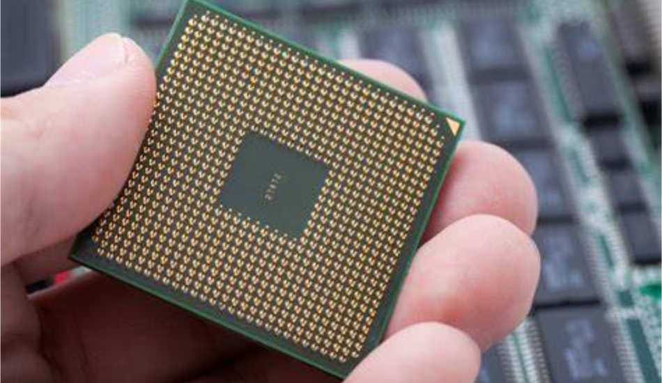
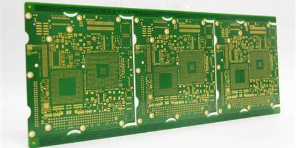
A printed circuit board (PCB) is the base for almost all electronics projects. It is made from fiberglass and has copper traces etched into it to connect different components. As electronic devices get more complex and compact, there is a need to fit more components into the same PCB space. This is where high density PCBs come in.
What is High Density?
High density in PCBs refers to having a higher component density per unit area compared to standard density boards. High density is enabled by:
Smaller Traces and Spaces
In a PCB, traces are the copper lines that connect different points, while spaces are the gaps between traces. By having thinner traces and smaller spaces between them, more traces can fit in the same area, allowing for more connections and components. Standard density boards have traces/spaces of 6/6 mil while high density boards can go down to 4/4 mil.
More Layers
Most PCBs have copper on the top and bottom layers. High density boards can have up to 12-16 layers. Components and connections can be placed across all layers, increasing useable area.
Smaller Vias
Vias are plated through holes that connect traces between layers. Using microvias with smaller diameters allows connections between layers without using as much space.
Higher Component Density
With the above improvements, more SMD components can be placed per unit area, compared to standard density. Component pin pitch can go down to 0.4mm.
Why Use High Density PCBs?

Here are some of the main reasons to use high density PCBs:
Miniaturization
The biggest driver is to make devices like cellphones and laptops thinner and lighter by squeezing more electronics in the same space. HDI technology enables further miniaturization.
Higher Performance
With shorter traces and compact design, high density boards offer better electrical performance with lower noise, crosstalk, and signal loss. This is useful for designs like ADCs, GPUs requiring high speed signals.
Lower Costs
By allowing higher component density per unit area, HDI PCBs can reduce the number of layers required, lowering costs. The more compact design also allows for smaller end products, reducing material costs.
Flexibility
The multilayer design provides more flexibility in routing complex connections between components in HDI PCBs. Difficult designs are easier to route.
Reliability
Despite higher component density, HDI manufacturing process ensures reliability is maintained through strict process controls.
HDI PCB Construction
High density PCBs achieve the high component density through the following design and construction techniques:
Stacked Microvias
Microvias with smaller diameters (0.1mm to 0.2mm) are stacked through multiple layers to form connections between non-adjacent layers. This allows high density routing while minimizing layer use.
![Stacked Microvias] (https://www.researchgate.net/profile/Yogendra-Mishra-2/publication/267324434/figure/fig3/AS:295816144191498@1447375701989/Build-up-HDI-technology-with-stacked-microvias-5.png)
Laser Drilling
Mechanical drilling cannot achieve the precision and accuracy needed for microvias in HDI PCBs. Laser drilling creates holes with diameters below 0.15mm, with positional accuracy of under 0.025mm.
Thin Core
Rather than using traditional 1.6mm FR-4 core, HDI PCBs use a thin core of 0.05mm to 0.2mm. This allows stacking more layers for increased component density, without greatly increasing thickness.
Tight Tolerances
HDI PCB fabrication requires holding tight tolerances of around 25μm for line width, annular rings, and other features. Automated optical inspection ensures tolerances are maintained.
Build-Up Layers
Build-up dielectric layers are coated on the core to embed the traces rather than etching them. This allows finer lines/spaces down to 2/2 mils to be achieved.
HDI PCB Design Guidelines
To fully utilize the benefits of HDI PCBs, engineers should follow these design guidelines:
- Use grid of 0.025mm for placing components and routing. Standard grid is too coarse.
- Minimize trace lengths for high speed signals. Keep lines short as possible.
- Match trace impedances for high speed signals using smaller widths.
- Use stacked microvias and blind/buried vias over through-hole vias.
- Use land patterns matched to component pins/balls, with 0.1mm annular rings.
- Minimize distance between decoupling capacitors and IC power pins.
- Use 2-4 plane layers for power and ground to reduce noise.
- Avoid 90 degree bends in traces. Use 45 degree bends when necessary.
- Allow 5:1 clearance between microvia and regular via.
- Plan ahead for thermal relief connections to inner plane layers.
HDI PCB Technology Comparison
There are several HDI technologies providing different capabilities:
Sequential Build-Up
Layers are built sequentially over the core using laser via drilling and copper electroplating. Multiple build-up layers can create high density routing over the core.
Modified Semi-Additive Process (MSAP)
A combination of subtractive and additive techniques creates the build-up layers over the core. Allows finer 8-10um lines and spaces.
Any Layer HDI
Uses stacked microvias and build-up dielectrics to allow routing between any two layers. Provides most flexibility for high density layouts.
2.5D HDI
Integrates multiple active die side-by-side on a high density substrate using microbump interconnections. Allows heterogeneous integration.
3D HDI
Active and passive die are stacked vertically using microvias and often with TSVs. Provides highest integration density but also highest cost.
HDI PCB Challenges
While HDI PCBs provide advantages, engineers should also be aware of the challenges:
- High fabrication complexity and cost due to tight tolerances.
- Requires advanced PCB fab equipment such as laser drills.
- Challenging for thermal management due to high power density.
- Complex and time consuming layout process.
- Difficult prototype and low volume production. Limited suppliers.
- Requires expertise in HDI design rules and constraints.
- Risk of decreased yields and reliability issues.
- Repair and rework is difficult or often infeasible.
- High frequency simulations essential to avoid signal integrity issues.
Applications of HDI PCBs
Some of the common application areas using high density PCB technology are:
Smartphones
HDI PCBs enabled smartphones to become thinner and lighter with more computing power. The boards integrate application processors, memories, RF circuitry, power management ICs, passives and other components in a very compact form factor.
Wearables
For smartwatches and fitness bands, HDI flex boards provide the ability to cram a surprising amount of functionality into a tiny curved space on the wrist.
Internet of Things
Miniaturized IoT sensors can be integrated into very small modules and packages using HDI PCBs to provide wireless sensing capabilities.
High Speed Communications
HDI provides the interconnection density and electrical performance required in 40/100 Gbps networking cards and routers supporting 5G infrastructure.
Automotive Electronics
Advanced driver assistance systems and infotainment solutions require HDI PCBs to fit multiple high performance ICs into limited dashboard space.
Aerospace and Defense
Ruggedized electronics for guidance, telemetry, radar and other applications use HDI boards due to their compact size, lower weight and ability to withstand vibration.
Summary
In summary, high density PCBs use smaller features, additional layers, microvias and build-up dielectrics to provide component densities up to 20-30x higher than standard boards. By enabling compact system designs with high electrical performance, HDI PCBs are crucial for modern portable and high speed electronics. However, they also bring design and fabrication challenges requiring specialized expertise. As electronics continue getting more sophisticated and compact, high density interconnection technology will only increase in importance.
Frequently Asked Questions
What are the key differences between HDI and conventional PCBs?
The main differences are:
- Trace/Space: HDI can go down to 2/2 mils vs 6/6 mils for conventional PCBs
- Microvias: HDI uses microvias with 0.1mm diameter vs 0.3-0.6mm for conventional
- Layers: HDI can have up to 20 layers vs typically only 2-8 layers for conventional
- Dielectrics: HDI uses build-up dielectrics while conventional uses core substrate
- Component Density: Up to 20-30x more components per unit area with HDI
What are the typical layer stacks used in HDI PCBs?
Some common layer stackups are:
- 4-6-4: 4 signal layers, 6 power/ground layers, 4 more signal layers
- 2-2-2-2-2: Alternating signal and power/ground layers
- 4-4-4-4: 4 signal layers spaced by 4 power/ground layers
High layer counts up to 16 or 20 are also possible with HDI.
Can conventional PCB assembly be used for HDI boards?
HDI PCB assembly requires specialized processes due to the small features and component densities:
- Tight component spacings require accurate high precision pick and place machines
- Microvias require controlled solder fill to avoid voids
- High density boards require advanced thermal management
- Fine pitch soldering down to 0.3mm pitch requires advanced methods
How are HDI PCBs tested after fabrication?
HDI PCBs require advanced testing such as:
- Automated optical inspection (AOI) for measuring trace widths, spacing
- X-Ray inspection to verify layer alignments and microvia interconnects
- Flying probe testing for electrical verification
- Impedance testing using TDR to match critical traces
- Functional testing of any embedded ICs
How much more expensive are HDI PCBs compared to conventional boards?
HDI PCBs typically cost about 4-5 times more than conventional PCBs of similar size. Exact pricing depends on:
- Number of layers
- Board thickness
- Material types used
- Quantity being procured
- Density and complexity of layout
So while HDI PCB fabrication has a higher cost, the benefits of miniaturization, performance and flexibility often justify the additional price.


Leave a Reply