Introduction
High density interconnect (HDI) printed circuit boards (PCBs) are advanced PCBs that enable denser interconnections and finer spaces between copper lines and pads. As electronic devices continue getting more compact and complex, HDI PCBs have become essential for many product designs.
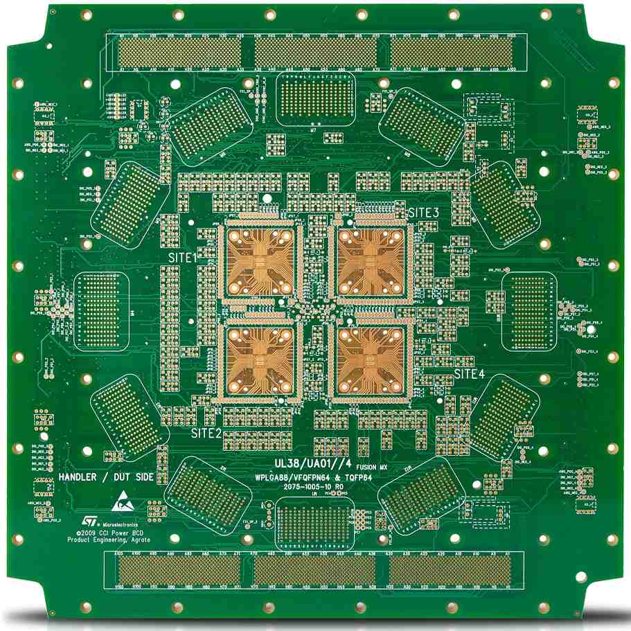
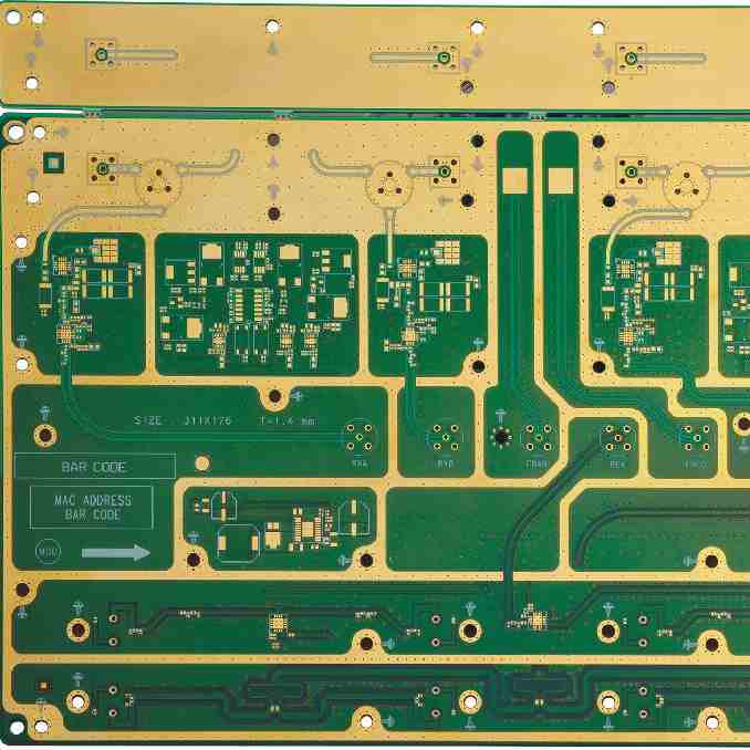
48 layer HDI PCBs represent some of the most advanced and intricate PCB solutions on the market today. With 48 layers, these boards can accommodate extremely dense circuit routing for complex devices. Selecting the right 48 layer HDI PCB manufacturer is critical to ensure high quality, reliable boards for your product.
This article provides an overview of 48 layer HDI PCB technology, key design and manufacturing considerations, and tips for selecting a capable 48 layer HDI PCB manufacturing partner.
What Are 48 Layer HDI PCBs?
HDI PCBs utilize finer lines and spaces, smaller vias, and thinner dielectric materials to increase circuit density compared to conventional PCBs. This enables more routing channels and layers in a compact form factor.
Key characteristics of HDI PCBs include:
- Line/space: Can be as fine as 10/10 μm (0.39/0.39 mil)
- Dielectric thickness: Can be as thin as 25-50 μm
- Microvias: Diameters can be as small as 25-60 μm
- Higher interconnect density
- More layers in a smaller z-axis height
48 layer HDI boards take these characteristics to the extreme with up to 48 copper layers interconnected using microvias. This allows extremely complex and dense designs all within a PCB thickness of just 0.8-1.6mm.
Applications of 48 Layer HDI PCBs
Due to their dense routing capabilities, 48 layer HDI PCBs are used for products like:
- High speed computing (server boards, supercomputers)
- Networking/telecom equipment
- Complex medical devices
- Advanced consumer electronics
- Aerospace/defense electronics
Any product with dense, high speed circuit requirements can benefit from the routing capabilities of 48 layer HDI PCBs. The boards provide more signal layers, power/ground layers, and isolation between critical nets.
48 Layer HDI PCB Design Considerations

Designing a 48 layer HDI PCB requires careful planning, simulation, analysis, and layout to leverage the benefits and avoid pitfalls. Here are some key design considerations:
Signal Integrity
With 48 layers of densely routed signals, maintaining signal integrity is imperative. Simulating routing networks, matching trace lengths, optimizing layer stackup, and assigning return paths are essential to prevent problems like crosstalk and reflections.
Power Integrity
Careful power delivery network (PDN) design including sufficient power and ground layers is needed to provide clean, stable power to devices. Decoupling capacitors must also be properly placed.
Thermal Management
HDI boards concentrate a lot of heat generation into a small form factor. Thermal analysis should be done to ensure adequate heat dissipation. This may require special materials like thermally conductive dielectric, copper planes as heat spreaders, and thermal vias.
Layer Stack Planning
The layer stackup must be planned to group similar signal types, isolate critical signals, and allow routing access between layers. This is a complex 3D puzzle.
Component Placement
Parts must be intelligently placed early in the design to enable efficient routing. High speed interfaces need to be routed first.
Manufacturing Limitations
The PCB manufacturer’s capabilities establish minimum line/space, via size, dielectric thickness, and other limits that must be accounted for.
With careful planning and design, a 48 layer HDI PCB design can successfully maximize routing density and performance.
48 Layer HDI PCB Manufacturing Process
Producing 48 layer HDI PCBs requires specialized manufacturing equipment, materials, and processes. Here is an overview of key fabrication steps:
Layer Stack Lamination
The core starts with a dielectric material such as polyimide laminated with copper foil. Additional dielectric and copper layers are sequentially laminated to build up the layer stackup. Registration is critical.
Drilling
Microvias just 25-60μm in diameter are drilled through the layer stack to interconnect layers. High precision laser or mechanical drilling equipment is required.
Metallization
The microvias and through holes are plated with copper to form the vertical interconnects between layers. Vacuum deposition or electroplating can be used.
Photolithography
The intricate wiring patterns are formed using photolithographic processes. Liquid photoresist is applied, exposed through masks, and then developed to form the circuit patterns.
Etching
The exposed copper is etched away to leave just the desired circuit traces and pads. Printed wiring channels down to around 10μm can be achieved.
Solder Mask & Legend Printing
Solder mask is applied over the entire board except areas to be soldered. Legend printing applies markings like component designators.
Testing
100% electrical testing validates connectivity and function. Automated optical inspection checks for defects.
Producing 48 layer HDI PCBs with acceptable yields requires specialized expertise and equipment. Not all manufacturers can build these boards reliably.
Tips for Selecting a 48 Layer HDI PCB Manufacturer
Here are some important factors to consider when choosing a 48 layer HDI PCB manufacturing partner:
Track Record with Advanced HDI
Look for manufacturers with a proven capability to produce the most advanced HDI boards reliably, not just standard multilayer boards. Ask for examples of complex HDI boards they have manufactured for reference.
Equipment and Processes
The manufacturer should have leading edge equipment like laser direct imaging and plating systems that can meet fine line/space and high layer count needs. They also need solid processes.
Quality Systems
Stringent quality control systems and testing are necessary, including automated optical inspection. Make sure quality certifications like ISO 9001 are in place.
Prototyping Capabilities
The ability to build small batches of prototype boards quickly is ideal for proving out designs. Ask about prototyping and low volume services.
Engineering Support
Experienced engineering support can help review designs for manufacturability and make recommendations if needed. Look for knowledgeable engineers.
Customer Service
Responsiveness to quotes, questions, and support issues is important. Make sure they value customer service.
With the right partner, 48 layer HDI PCB fabrication can be reliable and help bring advanced electronic products to market faster.
Frequently Asked Questions
Here are some common questions about 48 layer HDI PCB manufacturing:
What are the main benefits of 48 layer HDI PCBs?
The ultra high layer count and small features enable routing of very complex and dense designs not possible with conventional PCBs. 48 layer HDI boards provide more signal layers, isolation between critical nets, access to more power and ground planes, and miniaturization.
What are some key disadvantages of 48 layer HDI PCBs?
The main disadvantages are higher cost and complexity. The specialized materials, fabrication processes, and low yields increase costs. The designs are also very complex and require advanced engineering skills. Supply chain options are more limited.
What types of designs require 48 layers?
Very complex devices like high speed computers, servers, network switches, telecom gear, advanced radar and medical devices, and other products pushing the envelope of electronics miniaturization and performance need 48 layer HDI PCBs. Consumer products rarely need this capability currently.
What is the typical lead time for 48 layer HDI PCB prototypes?
Lead times can range from 10-20 days for a modest build of 10-50 pieces of a design already complete. For a new design, plan for 15-30 days to allow the manufacturer to review the design, order materials, and schedule production.
What types of lamination materials are used in 48 layer HDI PCBs?
Materials like polyimides (Pyralux) or bismaleimides (BT resins) are often used. These provide the combination of dimensional stability, dielectric properties, and heat resistance needed. Some boards may also incorporate special ceramic-filled dielectric layers.
Conclusion
48 layer HDI PCB technology enables revolutionaryrouting density, miniaturization, and performance for advanced electronics. While highly complex, following sound design practices and choosing the right manufacturing partner allows companies to leverage 48 layer HDI PCBs successfully. With smart utilization, 48 layer HDI PCBs will continue expanding the frontiers of electronic product capabilities.


Leave a Reply