High density interconnect (HDI) printed circuit boards (PCBs) that have 40 layers or more represent the cutting edge of PCB technology. They are used in advanced electronics applications that require extremely high component density, high speed signal integrity, and very complex circuit routing. Selecting the right 40 layer HDI PCB manufacturer is crucial to get high quality boards that meet your strict design requirements. This article provides an overview of 40+ layer HDI PCBs and what to look for when choosing a manufacturer.
What is a 40 Layer HDI PCB?
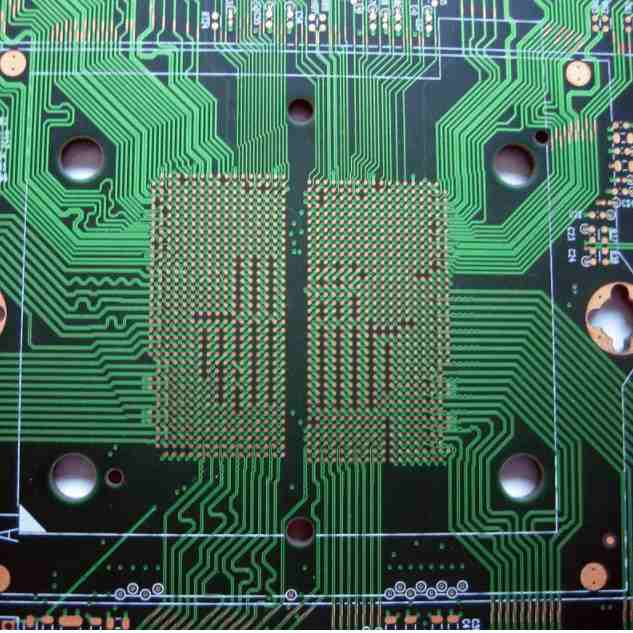
HDI PCBs use microvias and other advanced technologies to enable higher component density and more routing layers than conventional PCBs. Some key characteristics:
- Very high layer counts – 40 layers is on the high end but some HDI PCBs have over 60 layers.
- Thin dielectric layers – Dielectric layers are often ≤50 μm thick vs 100 μm on typical multilayer boards.
- Small vias – Microvias with ≤50 μm diameter connect layers instead of through hole vias.
- Fine lines and spaces – Trace widths and spaces down to ≤25 μm are common.
- High density component mounting – Allows placement of 0201 and 01005 sized surface mount parts.
Benefits of 40+ Layer HDI PCBs
The main benefits of high layer count HDI PCBs are:
- Increased routing density – More layers provides more routing channels for traces so components and routing can be packed tighter.
- Miniaturization – HDI technology enables smaller vias, lines, and component pitches leading to smaller overall board sizes.
- High speed performance – Thin dielectrics and dense power planes control impedances for high frequency signals.
- High pin count ICs – More layers provides more pin out capacity for large ball grid array (BGA) and land grid array (LGA) packages.
- Function Integration – Multiple circuits and functions combined onto one board.
These capabilities make 40+ layer HDI PCBs ideal for advanced applications like networking, telecom, defense, aerospace, and medical electronics.
40 Layer PCB Stackup
The layer stackup refers to the sequence of copper and dielectric layers in a multilayer PCB. Here is a typical 40 layer HDI stackup:<img src=”https://i.imgur.com/Kot7DmM.png” alt=”40 layer HDI stackup” width=”400″>
Key characteristics of a high layer count HDI stackup:
- Alternating dielectric and copper layers.
- Very thin dielectrics – typically ≤50 μm.
- Multiple high density routing sections with ≥16 layers each.
- Microvias connect the sections and route signals between layers.
- Buried and blind vias minimize via stubs.
- Many parallel power and ground planes.
- Thick outer copper layers – 70-200 μm for durability.
This stackup allows very high component densities exceeding 10,000 circuits per square inch.
Choosing a 40 Layer HDI PCB Manufacturer
Not all PCB fabricators can reliably produce 40+ layer HDI boards. Here are important capabilities to look for in a manufacturer:
HDI Experience
- Ask about their experience with high layer count HDI PCBs – at least 5 years is recommended.
- Request examples of prior 40+ layer boards they’ve produced.
- Ensure they regularly manufacture 20+ layer boards not just sporadic high layer prototypes.
Board Thickness Control
- Thickness uniformity is critical across the thin dielectrics in an HDI stackup.
- Look for layer uniformity tolerances ≤5-10 μm across the stackup.
- Ensure they measure thickness at multiple points on each board not just single point.
Registration Accuracy
- With microvias under 50 μm, highly accurate layer-to-layer registration is essential.
- Require registration capabilities ≤25-30 μm for reliable HDI boards.
Via Reliability
- The many microvias in HDI boards require superb plating quality to avoid reliability risks.
- Ask about their microvia plating defect rates – should be very low (<100 ppm).
- They should inspect 100% of microvia connections.
Advanced Testing
- 40+ layer boards require 100% electrical testing of nets, vias, and connections.
- Look for test coverage ≥95% of nodes and accessibility down to 25 μm features.
- Specialized tools like automated X-ray inspection of microvias.
Engineering Support
- There should be dedicated engineers to support DFM analysis and stackup design.
- Look for recommendations on optimal stackups, layer sequencing, and manufacturability.
By thoroughly vetting manufacturers on these parameters, you can identify capable partners able to deliver reliable, high yielding 40 layer HDI PCBs.
40 Layer PCB Design Considerations

To fully utilize a 40 layer board and enable your PCB manufacturer to fabricate it optimally, keep these guidelines in mind during layout:
Layer Sequencing
- Sequence signal layers between power and ground to control impedances.
- Avoid adjacent high speed layers to prevent crosstalk.
- Adjust stackup symmetry around the core for uniformity.
Split Planes
- Use multiple split power and ground planes in place of one thick plane.
- Allows channels for routing other signals within the plane layers.
Component Placement
- Mikli placement and make use of the full board area to maximize density.
- Group associated circuits together.
- Watch out for components blocking routing channels.
Board Outline
- Minimize irregular board shape which reduces panel utilization and can create supply chain issues.
- Discuss preferred outline and panel sizes with your manufacturer early in the design process.
HDI PCB Cost Considerations
As you might expect, 40+ layer HDI PCBs are more expensive than conventional multilayer boards. Here are some of the cost factors:
- Direct Costs – More layers means more materials, processing, and labor costs. You easily get into the thousands per board.
- Low Yields – Due to complexity, yields are lower, often 60-80% for high layer count boards. This means more scrap costs factored into pricing.
- Panel Utilization – Low volume complex boards utilize a panel much less efficiently. This wastes material and drives up cost.
- Qualification – More comprehensive testing and inspection is required, adding cost.
- CFPs – Complex, high mix boards often require custom test fixtures for electrically probing, which are expensive.
- Engineering Support – More engineering time is required for DFM analysis, stackup design, etc.
If designed properly however, you can maximize manufacturing yields for the lowest possible costs. This is where an experienced HDI PCB manufacturer contributes value through DFM guidance and process expertise.
Summary of Key Points
- 40+ layer count HDI PCBs enable very advanced electronics with high component density, fine features, and complex circuitry.
- Microvias, thin dielectrics, fine lines & spaces, and high layer counts allow far greater routing density than standard multilayer boards.
- Selecting a PCB manufacturer with proven HDI experience and capabilities is critical for success.
- Following DFM guidelines tailored for the board complexity enables the best manufacturability and cost structure.
As advanced electronics applications continue proliferating, demand for 40 layer and higher HDI PCB technologies will keep increasing as well. Partnering closely with a high capability manufacturer helps ensure you get these intricate boards produced successfully.
Frequently Asked Questions
What are some examples of products that use 40 layer PCBs?
40+ layer HDI PCBs are found in advanced electronics products including high speed switches, routers, and servers, radars and other defense electronics, satellites, MRI machines, DNA sequencing systems, and more. Generally, applications that require very high processing power, speed, or density utilize these complex boards.
What is the most number of layers achieved in an HDI PCB?
While most HDI PCBs range from 4-16 layers, some leading edge boards have exceeded 60 layers for extremely complex and dense designs. As interconnect densities keep improving, the layer counts will continue increasing.
Can flex PCBs have high layer counts?
Yes, rigid-flex PCBs can also utilize HDI technology and have 40+ layers. The rigid sections will have very high layer counts and component densities while the flex areas interconnecting them have fewer layers.
Does an entire 40 layer board need to be HDI?
No, a 40 layer board may contain conventionally stacked sections in addition to high density interconnect areas. The HDI technology would be utilized where maximum routing density and thin dielectrics are needed.
What design tools are used for 40 layer PCBs?
Advanced PCB design software like Cadence Allegro and Mentor Xpedition are typically used for 40+ layer HDI boards. They have extensive features for optimizing trace routing, plane design, 3D visualization, and DFM analysis on complex boards.


Leave a Reply