Introduction
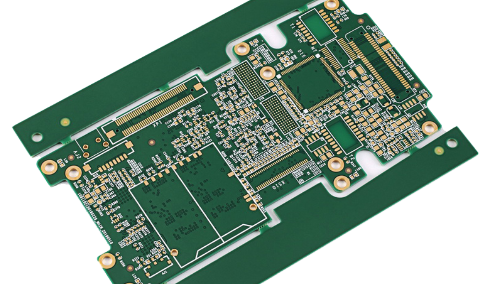
As electronic devices continue to get smaller and more complex, the printed circuit boards (PCBs) inside them must become denser and more intricate. This is where high-density interconnect (HDI) PCBs come in. HDI PCBs contain multiple layers – often 20 layers or more – with extremely fine traces and spaces, allowing for tighter component spacing and integration.
38 layer HDI PCBs represent the cutting edge of PCB technology. With 38 copper layers to work with, they provide unmatched routing flexibility for complex, miniaturized circuits. However, not just any PCB manufacturer can produce reliable 38 layer boards. Specialized expertise and advanced manufacturing capabilities are required.
In this article, we’ll look at key considerations when choosing a 38 layer HDI PCB manufacturer. We’ll explore the technical challenges involved in fabricating these boards and the qualifications you should look for in a potential supplier. Read on to learn how to select a partner who can deliver high-quality 38 layer HDI PCBs tailored for your product needs.
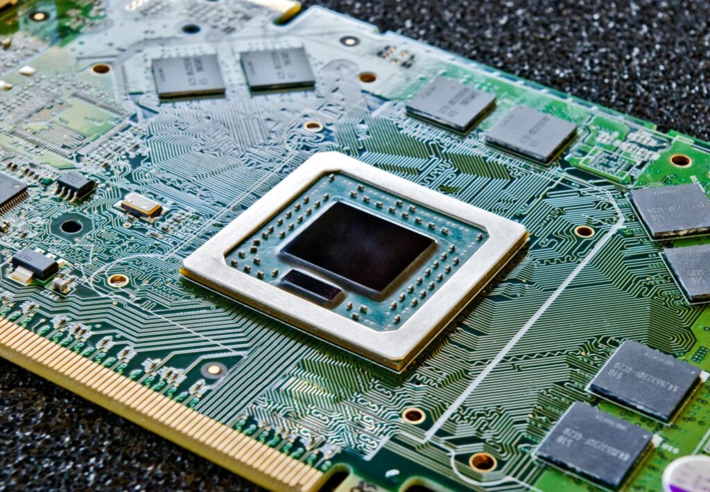
HDI PCB Manufacturing Capabilities
Building a 38 layer HDI PCB requires a whole suite of specialized fabrication techniques. Here are some of the advanced capabilities a qualified manufacturer must possess:
Laser Drilling
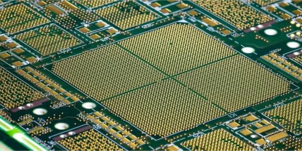
Creating thousands of interconnecting vias between layers demands precision laser drilling. The via holes on a 38 layer board can be as small as 25-50 μm in diameter. This is far below what standard mechanical drilling can achieve. Laser drilling provides the accuracy and repeatability needed at these miniature scales.
Plating Technology
After drilling, the many tiny vias must be plated with copper to form the interlayer connections. Advanced plating equipment is essential to achieving uniform metal deposition and complete via filling on a 38 layer board. At the same time, tight control of plating thickness is necessary to avoid Via bulging which can lead to poor connections.
Fine Line Fabrication
To fully utilize a 38 layer stackup, the manufacturer must be able to produce extremely fine traces and spaces. Line width/space down to 2/2 mil is typical on these boards. This requires advanced photographic, etching, and material processes tailored specifically for HDI manufacturing.
Layer Alignment
With so many layers, ensuring correct registration between layers is crucial. Any misalignment can cause open circuits and short circuits, rendering the board unusable. Maintaining tight layer-to-layer alignment tolerances is a must across the entire 38 layer stackup.
Lamination
Using specialized lamination processes, the layers of circuitry must be bonded together into a solid board. Eliminating voids or wrinkles within and between layers is critical. The lamination process must deliver a flat, uniformly bonded stackup.
Testing
Rigorous electrical testing and quality control steps are implemented by the manufacturer. This includes in-circuit testing, flying probe testing, automated optical inspection, x-ray inspection, cross-section analysis, and more. Ensuring each completed 38 layer HDI PCB meets spec is priority number one.
Qualifications of a 38 Layer PCB Manufacturer
To reliably produce quality 38 layer HDI PCBs, the manufacturer must have the right mix of experience, expertise, capabilities, and certifications. Here are the key qualifications to look for:
Years of Experience
Look for 10+ years fabricating HDI PCBs at high volumes. They should have a proven track record with satisfied customers relying on them for advanced HDI boards. The longer their experience, the more adept they are with the intricacies and nuances of HDI manufacturing.
In-House Capabilities
All the key fabrication processes should be handled in-house, including laser drilling, plating, oxide treatment, lamination, etc. Outsourcing steps can increase variability and uncertainty. Vertically integrated production allows for tighter process controls.
Engineer Expertise
The manufacturer should employ PCB engineers and technologists who live and breathe HDI. They should be capable of translating customer designs into manufacturable board stacks. Look for expertise in areas like signal integrity, thermal design, layer planning, etc.
Quality Certifications
Relevant quality management certifications include ISO 9001, ISO 13485, AS 9100, and IATF 16949. These demonstrate adherence to rigid quality systems covering all aspects of PCB fabrication. The highest reliability 38 layer boards come from ISO certified fabs.
UL and Defense Certifications
For boards destined for mission-critical applications, UL (Underwriters Laboratory) and defense certifications are key. These include UL 796 recognition and certification to MIL-PRF-31032, MIL-PRF-55110, and MIL-DTL-5541. Not all 38 layer manufacturers hold these specialized certifications.
HDI PCB Focus
Some PCB shops offer HDI boards but don’t specialize in them. Look for manufacturers 100% dedicated to HDI technology. Their equipment, processes, and expertise will be optimized specifically around high-density PCBs rather than standard multilayer boards.
Key Factors in 38 Layer PCB Fabrication
Producing a 38 layer HDI PCB is a complex undertaking with many steps from design to delivery. Here are some of the key factors the manufacturer must get right:
Stackup Design
The layer stackup provides the foundation. It must deliver signal integrity and impedance control while avoiding excessive lamination stresses. Collaboration between designer and manufacturer is ideal to optimize the stackup arrangement.
| Layer Type | Layer Count |
|---|---|
| Signal Layers | 32 |
| Dielectric Layers | 31 |
| Plating Layers | 2 |
| Total Layers | 38 |
Registration Accuracy
With over 15,000 vias to interconnect 38 layers, hole-to-land registration accuracy is paramount. Tight process controls during laser drilling, imaging, and lamination are needed to achieve tolerances of 0.100mm or better.
Base Material Selection
The resin chemistry and dielectric properties of the insulating base material chosen impacts electrical performance. Factors like low Dk and low Df are crucial for meeting impedance, loss, and speed requirements.
Via Stub Control
Minimizing via stub length by optimizing layer transitions is key. Excessive stub introduces reflections and signal distortion. Stub control throughout the layer stackup ensures signal integrity across the full frequency spectrum.
Copper Balance
Careful layer planning maintains copper balance across the board thickness. This avoids internal stresses leading to warpage or delamination. Achieving copper symmetry of <5% panel thickness is standard for a quality 38 layer HDI PCB.
Improved Yields
With a 38 layer board, a single defect anywhere can require scrapping the entire panel. The manufacturer must utilize processes that lower defects and improve yields – precision drilling and imaging, cleanroom assembly, automated inspection, etc.
Key Applications of 38 Layer HDI PCBs
Some of the key application areas where 38 layer HDI PCB technology provides benefits:
- Smartphones – Routing flexibility allows integrating more features into ultrathin, high-performance smartphones.
- Wearable Technology – 38 layers allow complex functionality within extremely small wearable product footprints.
- Medical Devices – Miniaturized designs meet the tight space and performance needs of implantable and wearable medical devices.
- Defense/Aerospace – Rugged 38 layer boards meet reliability requirements under challenging operating conditions.
- Automotive – HDI PCBs help consolidate many standalone systems into integrated body controllers and infotainment systems.
Within these areas, specific applications include but aren’t limited to:
- Radar systems
- Wireless communications infrastructure
- GPS navigation
- Patient monitoring systems
- Engine control units
- Battery management systems
- Avionics equipment
- Mission computers
Key Questions to Ask a Potential Manufacturer
If you’re looking to have 38 layer HDI PCBs made, here are some key questions to ask potential manufacturers:
- How long have you been manufacturing HDI PCBs, and what percent of your overall business do they represent? You want long experience and specialization in HDI.
- What is the minimum trace width and space you can achieve? They should be able to do 2 mil lines and spaces or less.
- What is your laser drilling diameter capability? Look for 25-50 μm vias or below.
- Do you meet defense and aerospace certification requirements? If needed, target manufacturers with credentials like MIL-PRF-31032 or MIL-PRF certification.
- Can you optimize layer stackups based on electrical performance needs? They should offer stackup design services.
- How do you ensure accuracy across all 38 layers? Ask about their process and tooling for registration control.
- What test and inspection methods do you use to ensure quality? Look for x-ray, automated optical inspection, cross-sectioning, and more.
- Can you provide relevant references or sample customers? Reputable manufacturers will share success stories.
Conclusion
As PCBs continue getting denser and more complex, 38 layer HDI boards provide the interconnectivity needed to drive miniaturization across many advanced electronics segments. However, realizing the benefits requires a PCB manufacturer equipped with specialized expertise and capabilities in HDI fabrication. They must achieve precisions down to microns across a 38 layer stackup. By selecting a qualified partner, you can get high-performing 38 layer HDI PCBs tailored to your product needs.


Leave a Reply