Introduction
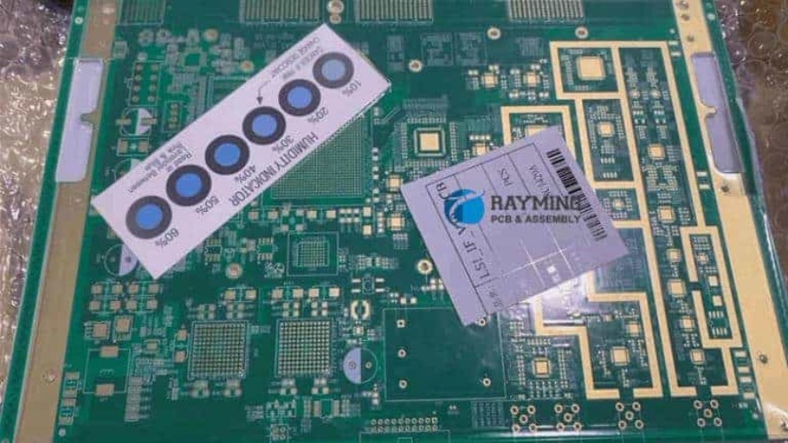
High density interconnect (HDI) printed circuit boards (PCBs) are complex multilayer circuit boards with fine lines, spaces and high connection pad densities. They enable integration of advanced semiconductor packaging and interconnect technologies for products that require high speed, high density and reduced weight and size.
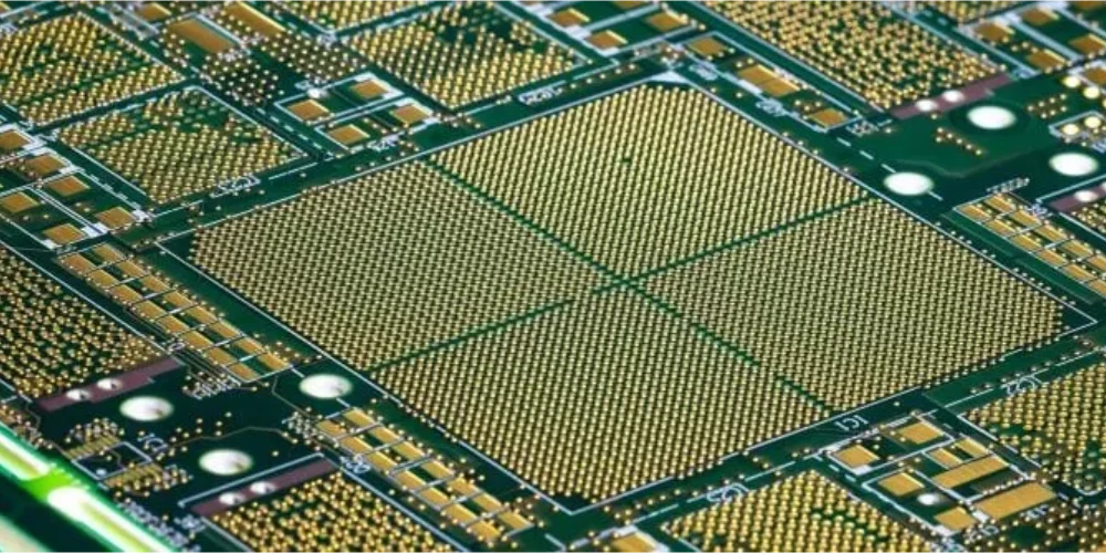
HDI PCBs with 36 layers represent the cutting edge of PCB technology today. They pack trace widths and spacings down to 2 mils with up to 20-25 mil thick circuit boards. This allows a massive increase in interconnect density and component mounting.
As a result, 36 layer HDI PCBs are increasingly being used in advanced electronics like servers, telecom infrastructure, aerospace avionics and medical devices where performance, reliability and precision are paramount. However, sourcing and qualifying reliable 36 layer HDI PCB manufacturers can be challenging.
In this guide, we will cover the key factors to consider when selecting a 36 layer HDI PCB manufacturer.
What are the typical applications of 36 layer HDI PCBs?
Some of the common applications that utilize 36 layer HDI PCB technology include:
- High speed computing systems like enterprise servers, data centers and supercomputers
- Networking and telecom infrastructure equipment like routers, switches and base stations
- High density interconnects for avionics systems in aerospace applications
- Advanced medical diagnostic and imaging equipment
- High precision test and measurement equipment
- Complex industrial automation systems
The ultra high wiring densities and interconnect performance make 36 layer HDI PCBs ideal for these types of advanced electronics applications. The circuits enable complex designs with high component counts to be integrated into relatively compact form factors.
Key Capabilities for a Reliable 36 Layer HDI PCB Manufacturer
When evaluating potential manufacturers for 36 layer HDI PCB prototypes or volume production, here are some of the key supplier capabilities to look for:
1. Proven HDI and Multilayer Technology
The manufacturer should have an established track record of manufacturing high layer count PCBs utilizingSequential Build-Up (SBU) and High Density Interconnect (HDI) technologies. They should be able to demonstrate experience with handling ultra-thin core boards, microvias, fine lines/spaces and strict impedance control.
2. Engineering Support
The supplier should have knowledgeable engineering resources to support the design process. This includes providing recommendations around optimal stackups, layer sequencing and maintaining signal integrity across 36 layers.
3. Rigid-Flex PCB Capability
Many advanced HDI board designs involve rigid-flex PCB configurations to integrate multiple PCBAs and components. So look for suppliers with proven expertise in rigid-flex PCB fabrication.
4. Miniaturization and Packaging
To fully utilize the capacities of a 36 layer board, the PCB design is likely to require advanced IC packaging (e.g. BGA), high density fine pitch connectors and buried/blind vias. The manufacturer should demonstrate these capabilities.
5. Advanced Testing
Verify that the supplier can conduct testing for high speed signal integrity and power integrity across all layers. This includes microwave testing, TDR/TDT analysis and full bed-of-nails testing for boards with 20mil thickness.
6. Precise Process Controls
Fabricating 36 layer HDI PCBs requires extremely tight process controls to repeatedly produce boards without defects. The manufacturer should have strict statistical process control andOperators ready to intervene if any process deviates from Six Sigma quality standards.
7. Manufacturing Scale
The supplier should have sufficient operational scale (e.g. multiple SBU lines) and manufacturing capacity to produce high layer count HDI boards in required quantities without compromising lead times or quality.
Comparing Top 36 Layer HDI PCB Manufacturers

Many PCB manufacturers claim to support 36 layer HDI boards. However, only a few have the technical capabilities, engineering expertise and manufacturing infrastructure to reliably deliver such complex boards.
Here is an overview of some of the top 36 layer HDI PCB manufacturers to consider:
| Manufacturer | Location | Core Capabilities |
|---|---|---|
| TTM Technologies | US, Asia | – 20+ HDI lines globally<br>- 50 board thickness capability <br>- Rigid-flex expertise |
| AT&S | Europe, Asia | – 30 layer HDI boards <br>- Flex/rigid-flex PCBs <br>- Aerospace certifications |
| Tripod Technology | Taiwan | – 36 layer HDI boards <br>- 2 mil L/S capabilities <br>- Quick turn prototypes |
| Unimicron | Taiwan | – 16 layer SBU line <br>- Advanced HDI package <br>- High mix/low volume |
| Isola | Global | – Multilayer laminate expertise <br>- Extensive HDI materials range <br>- Technology leader |
TTM Technologies
With over 20 HDI lines across Asia and North America, TTM Technologies is one of the largest and most recognized PCB manufacturers globally. The company has fabricated boards with over 50 layer counts and claims to be the world leader in HDI technology.
TTM also has specialized expertise in rigid-flex PCBs ideal for advanced multilayer boards used in aerospace, defense, telecom infrastructure and medical applications. Their in-house engineering team supports complex designs including impedance modeling and signal integrity simulation.
AT&S
AT&S is a European PCB manufacturer known for its advanced HDI and IC substrate capabilities targeted at high reliability applications. Their plant in Austria produces HDI boards with up to 30 layers, 3mil line/space and 100μm microvias.
They are accredited to supply multilayer boards for the defense and aerospace sectors. AT&S also has a strong technology focus on flexible printed circuits, rigid-flex boards and RF/high frequency PCBs.
Tripod Technology
Based in Taiwan, Tripod Technology has ramped up investment in HDI and hyperdensity board production over the past decade. They are now able to manufacture 36 layer HDI boards in small to medium volumes with 2 mil line and space.
Tripod is especially competitive for providing fast turnaround prototypes and new product introduction (NPI) volumes for advanced multilayer HDI boards. They also design and fabricate package substrates for flip chip and other advanced IC packaging.
Unimicron
Unimicron is a major PCB manufacturer in Taiwan with a 16 layer sequential buildup (SBU) line focused on advanced HDI boards. They offer a complete HDI package including IC substrate core fabrication, microvia filling/hole making and mixed embedded passives.
They specialize in high mix, small-to-medium volume runs which matches well with NPI volumes for new multilayer board introductions. Unimicron also has expertise in heavy copper, blind/buried vias and IC substrates.
Isola
While not a full-service PCB manufacturer, Isola is a core laminate and prepreg material supplier for multilayer PCBs globally. Their polymer laminates are used in the majority of advanced HDI boards up to 36 layers and beyond.
Isola has an extensive materials portfolio engineered to meet the demands of higher speeds, higher temperatures and higher densities in next-gen multilayer boards. They co-develop solutions with leading HDI PCB manufacturers worldwide.
Key Factors When Sourcing 36 Layer HDI Boards
Here are some important considerations when sourcing production volumes of 36 layer HDI PCBs once you have qualified suppliers:
Lead Times
Expect longer lead times for engineering, prototyping and manufacturing of 36 layer boards. Engage suppliers early and plan for 8-12 week initial production lead times.
Supply Chain Protection
Diversify component sources and suppliers for critical board materials to hedge supply chain risks. There are fewer alternate sources once you reach the bleeding edge of HDI board technology.
Cost
While not inexpensive, the costs of advanced 36 layer HDI PCBs have come down considerably as manufacturing experience increases. Look for suppliers that offer cost transparency and work to drive down costs through design optimization and process improvements.
Quality
Zero defects are critical. Rigorously qualify manufacturers, builds in compliance matrices focused on verification, statistical process controls, testing and inspection.
Data Security
Require suppliers to demonstrate data security especially when dealing with sensitive intellectual property (IP) inherent in leading edge PCB designs.
Packaging and Distribution
With large, ultra-thin boards, careful packaging, handling and ESD precautions are a must. Ensure the manufacturer has rigorous procedures in place.
Lifecycle Management
Plan for multiple board revisions and define processes to manage BOMs, configuration control and part obsolescence through the entire product lifecycle.
Frequently Asked Questions
Q: What are the key benefits of 36 layer HDI PCB technology?
A: The ultra-high wiring densities and layer counts enable far greater interconnectivity and component mounting density. This allows for miniaturization, performance improvements, weight reduction and functional integration that is not possible with conventional PCB technologies.
Q: What are the typical design rules for trace widths and clearances on 36 layer boards?
A: Most 36 layer designs utilize 2 mil trace/space paired with 1 mil/1 mil vias. However, some industry leaders can achieve 1 mil line widths and spaces. Microvias are typically 100μm. Total board thickness is typically 20-25 mils.
Q: What types of materials are used as dielectric laminates in 36 layer HDI boards?
A: Typical dielectric materials include polyimides (PI), bismaleimides (BT), FR-4, Rogers laminates and Isola high performance thermoset resins. Laminate materials are engineered for stability, low moisture absorption, thermal endurance, adhesion and electrical performance.
Q: How are microvias created on HDI boards with 36 layers?
A: Microvias are typically laser drilled and then plated/filled to connect traces across layers. The limit is around 100μm vias but laser direct imaging can achieve 75μm and smaller microvias. The process requires high precision lasers and plating equipment.
Q: How are 36 layer HDI boards tested and inspected during manufacturing?
A: 100% electrical testing validated design functionality. Automated optical inspection looks for physical defects. Signal integrity testing verifies acceptable high speed performance. Bed-of-nails and flying probe testing validates connections between all layers.
In summary, 36 layer HDI PCB technology represents the leading edge of multilayer boards, enabling highly complex designs and miniaturization. Carefully qualifying manufacturers based on proven HDI expertise, engineering capabilities and manufacturing quality is key to success. This technology will continue advancing as the demand for high-performance electronics grows in aerospace, defense, telecom infrastructure, data centers and advanced medical devices.


Leave a Reply