
Introduction
As electronic devices become more complex and compact, there is an increasing need for printed circuit boards (PCBs) that can accommodate more layers and finer features. A high-density interconnect (HDI) PCB with 32 layers represents the cutting edge of PCB technology, packing interconnects and traces into a remarkably small space. In this article, we will examine the capabilities of 32-layer HDI PCB manufacturers, the benefits of using a board with so many layers, and the challenges involved in reliably producing them.
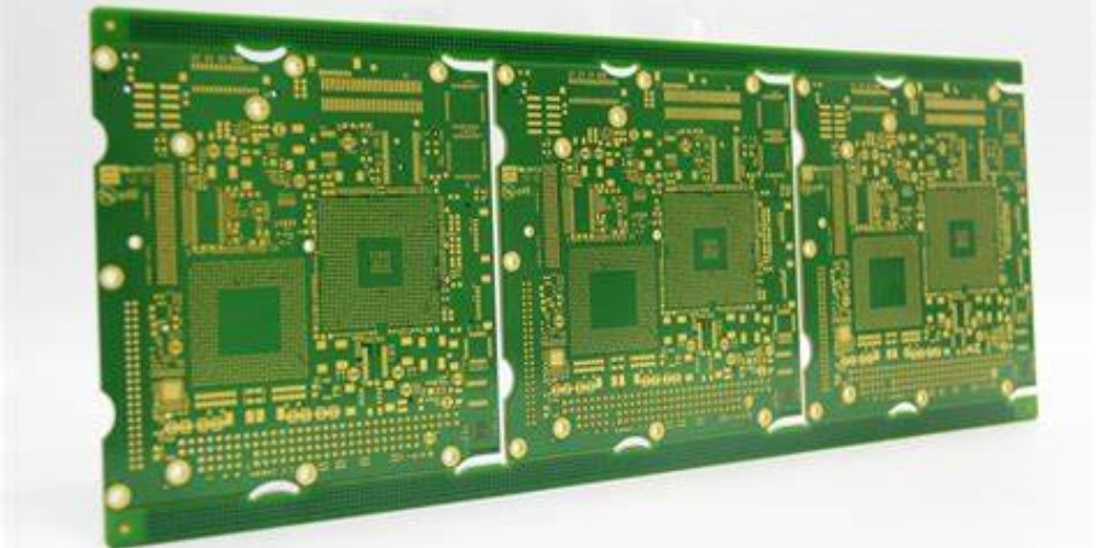
What is a 32 Layer HDI PCB?
A 32 layer PCB contains, as the name suggests, 32 conductive copper layers interleaved with dielectric material. Vias make electrical connections between the layers. Here are some key characteristics of a 32 layer HDI PCB:
- Extremely dense interconnects down to 20-25 μm line width and gap.
- Stack-up with build-up dielectric layers, often using low-loss materials.
- Large number of microvias (≤50 μm diameter) for layer-to-layer connections.
- Finer features than conventional PCBs.
- More routing channels allows greater flexibility.
- Overall thickness under 1 mm.
By comparison, a standard multilayer PCB rarely exceeds 16 layers and has larger features and spaces between traces. HDI technology allows far greater interconnect density.
Benefits of 32 Layer HDI PCBs
The main benefits of boards with more layers include:
- Miniaturization – More layers in a smaller space allows for smaller and thinner end products.
- Increased functionality – The extra layers make room for more signals and circuitry.
- Higher speeds – Finer traces and spaces allow higher frequency signals.
- Efficient power distribution – More power and ground planes manage voltage drops.
- Signal integrity – Careful stack-up and layer placement control impedance.
- Flexibility – More routing channels leave plenty of design options.
In essence, HDI PCBs provide the highest interconnect density and performance for advanced electronics. The 32-layer stack-up offers ample space for routing complex devices.
Capabilities of a 32 Layer PCB Manufacturer
Building reliable HDI PCBs with 32 layers requires expertise across the entire manufacturing process:
Superior Equipment
- Photolithography – High-end mask aligners and direct imaging can achieve line width/spaces down to 20 μm or less.
- Laser drilling – Precise laser systems drill small microvias (≤50 μm) through multiple layers.
- Plating and etching – Equipment must plate uniform copper and precisely etch fine features.
- Lamination – Layer-to-layer registration accuracy of 5 μm or better.
- Automated optical inspection (AOI) – Inspects accurate trace sizes, positioning, etc.
- Electrical testing – Tests for continuity, shorts, and functionality at multi-GHz speeds.
Materials Expertise
- Dielectrics – Thin cores and build-up materials with tight dialectric tolerances.
- Copper foils – Very thin foils down to 3-5 μm in thickness.
- Prepregs – Tight control of resin content and flow.
- Via fill – Copper-filled and capped microvias.
Process Capabilities
- Layer-to-layer registration and alignment.
- Thin core handling and lamination.
- Sequential build-up process.
- Surface finishes down to 0.5 μm roughness.
- desmear and etchback of microvias.
- Plating small vias and holes.
Quality and Testing
- First pass yield minimizes rework.
- AOI, x-ray, and electrical testing.
- Coupon design to confirm tolerances.
- Focus on continual improvement.
Advanced Certifications
- AS9100 – Aerospace quality management.
- ISO 9001 – Quality management.
- IPC 6012DS – HDI qualification.
- IPC Class 3 capability.
Only manufacturers that can demonstrate all of these capabilities will be able to reliably produce high yields of 32 layer HDI PCBs.
Challenges in Manufacturing 32 Layer HDI PCBs
While having 32 layers provides valuable design benefits, it creates some significant manufacturing challenges including:
- Registration accuracy – Aligning 32 layers requires precision equipment and process control.
- Via reliability – Plating small microvias through multiple layers is difficult.
- Lamination – Bonding so many thin dielectric layers and copper sheets.
- Fabrication defects – More layers means more chances for faults to occur.
- Testing – Verifying boards with hidden vias and traces.
- Yield – Achieving high yields is critical due to high costs.
These challenges make it imperative to choose a PCB manufacturer with proven experience fabricating 32-layer HDI boards. They need advanced equipment, tight process control, and engineering expertise to be successful.
Leading 32 Layer PCB Manufacturers

Many PCB manufacturers claim to offer HDI capabilities. However, only a few have the specialized expertise to reliably produce 32-layer HDI boards cost effectively. Here are some of the leading manufacturers of 32 layer PCBs:
TTM Technologies
One of the largest PCB manufacturers in the world, TTM offers 32 layer HDI boards with line width/space down to 15 μm. Their interconnect density capability reaches up to 60,000 traces per square inch. They utilize laser drilled microvias as small as 25 μm.
AT&S
Headquartered in Austria, AT&S produces 32 layer boards with 20 μm traces and spaces. They use a specialized sequential lamination process and can incorporate buried capacitance layers. Many of their customers are in high reliability aerospace and defense industries.
Tripod Technology
Based in Taiwan, Tripod is a major producer of HDI boards capable of 16-28 layer stackups. They use laser microvia drilling and low-loss dielectric materials. Tripod’s process integrates stacked microvias for increased interconnection density.
Unimicron
Also based in Taiwan, Unimicron offers build-up board technology for multilayer HDI PCBs. They can produce flex-rigid boards with built-in connectors. Unimicron emphasizes their vertically integrated process for quality control.
Würth Elektronik eiSos
This European manufacturer has facilities in Germany. They produce multilayer boards with 30 μm line widths and microvias. Würth uses special equipment to drill ultra-small vias just 40 μm in diameter.
Choosing a 32 Layer PCB Manufacturer
Here are some tips on selecting a 32 layer HDI PCB manufacturer:
- Review their HDI and microvia capabilities. Ask for technology roadmap.
- Make sure they can demonstrate certified quality systems.
- Request HDI-specific qualifications like IPC 6012DS.
- Ask for examples of 32+ layer boards recently produced.
- Evaluate their first pass yield and defect rates.
- Ensure they have qualified HDI materials technology.
- Check capabilities for high-speed design, signal integrity, and EMC.
Conclusion
As devices require increased functionality in ever-smaller packages, PCBs with 32 copper layers or more become essential. Leading HDI PCB manufacturers can reliably produce these boards with fine features to integrate complex circuitry. By utilizing cutting-edge manufacturing processes, advanced equipment, and specialized materials, they overcome the difficulties inherent in fabricating boards with so many layers. Choosing an experienced partner helps ensure your next 32 layer HDI PCB design can be expertly manufactured with high yields.
FQA
What is HDI technology?
HDI stands for high-density interconnect. It allows PCBs to have finer traces, smaller spaces between conductors, and microvias under 100 μm in diameter. This enables greater interconnect density.
What are some key benefits of a 32 layer PCB?
A 32 layer HDI PCB provides more routing layers for increased functionality, allows for smaller and thinner end products, supports higher speed signals, and offers superior power distribution and signal integrity.
What line width/space is achievable on a 32 layer board?
Leading 32 layer PCB manufacturers can achieve line widths and spaces down to 20 μm or sometimes even finer. This represents the limits of conventional PCB photolithography.
Why is it difficult to reliably manufacture 32 layer HDI boards?
The challenges include precisely aligning all the layers during lamination, drilling the high density of microvias, achieving high first pass yields, and electrically testing the finished boards when vias and traces are buried.
What certifications should a 32 layer PCB manufacturer have?
Relevant certifications include IPC 6012DS qualification, IPC Class 3 fabrication, ISO 9001 quality management, and AS9100 aerospace quality systems. These validate their capabilities and process controls.


Leave a Reply