High-density interconnect (HDI) printed circuit boards (PCBs) are an advanced technology that allows for higher component density and more complex circuitry than standard PCBs. HDI PCBs have several key advantages for designers:
Benefits of Using HDI PCBs
HDI PCBs provide a number of benefits compared to standard PCB technologies:
- Higher component density – The stacked vias and microvias of HDI allow for placing components closer together, supporting advanced component packaging methods. This enables smaller and lighter end products.
- Miniaturization – HDI’s fine features and spacing mean circuits can be condensed into a smaller physical space. This facilitates compact or portable product designs.
- Higher signal speed – The tightly spaced traces, vias, and components of HDI provide shorter signal paths. This means signals can propagate faster through the board.
- Noise reduction – Ground planes and power planes can be placed closer to signals, which helps minimize noise. This enables reliable high-speed signals.
- Routing flexibility – Microvias allow connections between layers that bypass adjacent layers. This provides more routing options to connect components efficiently.
- Lower costs – By reducing PCB layer count, HDI can lower production costs and material requirements. The miniaturization also means reduced hardware sizes and costs.
HDI PCB Technology Overview
HDI PCBs achieve their high component density through advancements in via structures and trace dimensions:
- Microvias – Smaller laser-drilled vias with diameters typically under 150 μm (but sometimes as low as 50 μm). Allow connections between layers without requiring surface pad stacks.
- Stacked vias – Offset stacked vias that connect to different layers to save surface area.Replaces surface pad stacks.
- Thin dielectrics – dielectric layer thicknesses under 75 μm, allowing for tighter layer spacing. Common materials include polyimides and liquid crystal polymers.
- Fine line traces – Trace/space dimensions under 100 μm facilitates component miniaturization and high-density routing. Requires advanced processes like laser direct imaging (LDI).
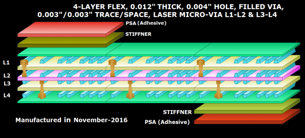
HDI PCBs commonly have 4-8 stacked microvia layers connected by a thicker “core” dielectric layer. This hybrid construction provides a balance of HDI’s benefits while controlling costs and manufacturability.
HDI Design Rules and Constraints
While HDI provides many benefits, the tight dimensions also impose constraints. Designers should follow HDI-specific guidelines:
Minimum Trace/Space Widths
The thin trace widths demand increased spacing rules to prevent shorts:
| Trace Width | Minimum Space |
|---|---|
| ≥ 75 μm | 75 μm |
| ≥ 50 μm | 50 μm |
Minimum Annular Rings
Annular rings around microvias should meet the fabricator’s specfication, often ≥ 50 μm. This ensures a reliable connection.
Microvia Capture Pads
Capture pads provide sufficient landing area and annular ring margin for the microvia barrel:
- Recommended capture pad diameter is ≥ 120 μm
- Capture pads can overlap plane layers if isolated by a 6-8 μm dielectric gap
Microvia Placement
- Stagger adjacent microvias at least 150 μm apart to prevent fracturing the thin dielectric layers
- Keep ≥ 50 μm distance from embedded component pads
Plane Layers
- Reference planes should be ≤ 60 μm thick to control layer stack height
- Multiple thick plane layers can be integrated using stacked/staggered vias
HDI Materials and Fabrication Considerations
HDI PCBs demand advanced materials and fabrication processes to produce their fine features reliably.
Dielectric Materials
Common dielectric materials include:
- Polyimides – High thermal stability for multilayer boards. Allows thin laminations. E.g. HD-4000 series.
- Liquid crystal polymer (LCP) – Extremely low loss, stable dielectric. Withstands multilayer lamination pressures. E.g. R/flex 4000 series.
- PTFE composites – Reinforced for dimensional stability. Lower loss than FR-4. E.g. high-frequency materials like Rogers RO4000 series.
Copper Foil
Very thin rolled annealed copper foils, such as 3-5 μm thickness, are preferred for fine traces. This helps improve etching of fine lines.
Laser Processing
Small microvias and fine traces are fabricated using laser imaging rather than traditional lithographic methods:
- Laser direct imaging (LDI) patterns microvias/lines by selective laser ablation. Allows high-precision small features.
- UV laser drilling creates microvias, often ≤ 75 μm diameter. Allows high density via placement.
Layer Alignment
Thin layers demand precise laser alignment systems to control layer-to-layer registration. Tight alignments minimize via annular rings.
Surface Finishes
HDI boards often use organic solderability preservative (OSP) rather than immersion tin or gold finishes. OSP does not require electroplating.
HDI Stackup Design
The stackup design defines the layer structure of the HDI PCB. This impacts manufacturability, signal and power integrity, and product performance.
Layer Count
HDI designs typically have 4-12 conductive layers to balance density, performance, and fabrication complexity. Some key factors:
- Routing density – More layers provide additional routing channels for dense, complex circuity.
- Signal integrity – Additional layers allows reference planes next to critical signals to control impedance and reduce noise.
- ** manufacturability** – Each layer adds process steps of lamination, drilling, etc. Yield and cost increase.
- Board thickness – Added layers increases thickness. Can impact end product size.
Core Thickness
The thicker core dielectric provides mechanical stability, while thin dielectrics are used for the HDI stackup:
- Core thickness is often 200-400 μm
- Total thickness with HDI buildup is typically ≤ 1 mm
Layer Sequence
Typical HDI layer sequence:
- Signal layers in HDI buildup region
- Thick core dielectric
- Buried reference plane layers
- Additional signal layers
Signals route through microvias in the HDI layers. Signals crossing core layer use stacked vias.
HDI Design and Analysis
HDI PCB design requires attention to signal and power integrity to ensure performance. Simulation tools and design guidelines are key.
Signal Integrity
Thin dielectrics and tight traces can impact impedance control and propagation:
- Use impedance calculators to design controlled-impedance traces meeting target ±10%
- Employ 2D extraction tools to simulate actual trace impedance
- Model vias, plane gaps as discontinuities affecting propagation
- Match transmission line length or add termination resistors to control reflections
Power Integrity
HDI power delivery requires attention to PDN impedances:
- Use multiple via pairs and capacitors to provide charge locally and reduce inductance
- Keep reference planes clear of splits and gaps which increase impedance
- Model plane cavity resonances; add capacitor damping if needed
- Consider embedded thin-film power cores or buried capacitance materials to augment power distribution
Thermal Analysis
The dense component layout impacts heat dissipation:
- Use thermal modeling software to simulate operating junction temperatures
- Ensure sufficient copper heat spreader layers to conduct heat
- Incorporate thermal vias to connect layers and improve vertical heat conduction
Manufacturing HDI PCBs
HDI PCB fabrication requires advanced processes, materials, and precise process control. Here is a general fabrication overview:
Inner Layer Production
- Apply photoresist dry film and expose with LDI for circuit patterning
- Etch roll-annealed thin copper foils to form fine conductors
- Clean and prepare layers; apply dielectric bonding films
Layer Lamination
- Align dielectric films and circuit layers using laser registration
- Laminate layers under vacuum pressure using thermal compression or autoclave
Microvia Formation
- Use UV laser to ablate holes through dielectric at precise locations
- Apply chemical processes to clean and activate hole walls for plating
Outer Layer Processing
- Build up copper on exterior layers using semi-additive plating
- Pattern outer layers using photolithography and copper etching
Drilling and Plating
- Mechanically drill larger holes for component holes and thicker vias
- Electroplate copper to plate through holes, microvias, and exterior surfaces
Solder Mask and Finishing
- LDI define solder mask openings for pads and traces
- Apply solder mask ink; cure; clean
- Apply OSP surface finish to exposed metals
HDI Design Guidelines Summary
In summary, following are some key guidelines for a successful HDI PCB implementation:
- Use minimum trace widths and spacings per fabrication capabilities
- Follow annular ring rules for all microvias
- Provide sufficient capture pads for each microvia
- Stagger adjacent microvias to prevent dielectric fracturing
- Incorporate reference planes next to critical signals
- Minimize splits and gaps in reference planes
- Model signal and power integrity to ensure performance
- Include thermal analysis and management provisions
- Use qualified and experienced HDI fabrication vendors
Frequently Asked Questions
What are the key benefits of using HDI PCB technology?
The main benefits of HDI PCBs are:
- Higher component density from microvias and fine features
- Miniaturization from tight spacing and thin dielectric layers
- Improved signal speed through shorter, optimized routing
- Lower noise by incorporating more reference planes
- Greater routing flexibility with microvias between layers
- Potential lower costs through PCB miniaturization
How small can microvias be?
Microvia diameters typically range from 75-150 μm, though laser drilling can produce holes as small as 25-50 μm in some cases. The lower limit depends on fabrication capabilities. Smaller microvias allow greater via densities.
What design tools are used for HDI PCBs?
HDI designs utilize the following specialized tools:
- Impedance calculators to design controlled traces
- 2D field solvers to extract actual trace impedance
- Signal integrity simulators to model time/frequency behavior
- Power integrity tools to simulate plane currents and PDN impedance
- Thermal modeling software to simulate heat dissipation
Advanced PCB layout tools also help enable the complex routing and high component densities.
What fabrication processes are critical for HDI?
Key fabrication processes include:
- Laser direct imaging (LDI) of lines/spaces under 100 μm
- UV laser drilling to make microvias under 150 μm diameter
- Thin copper foils, 3-5 μm, to support fine traces
- Thin dielectrics, ≤ 75 μm, to allow tight layer stacks
- Laser registration for precision layer-to-layer alignment
How many layers are typical for HDI designs?
A typical HDI design uses 4-8 thin dielectric layers with microvias, sandwiched around a thicker core dielectric layer. Total layer counts are usually 8 layers or greater. More layers are possible but increase complexity.
The HDI layers provide routing channels and allow high-density component placement. The thicker core provides mechanical stability.


Leave a Reply