Introduction to Printing Resolution
Printing resolution is a crucial factor when it comes to the quality and precision of printed electronic components. In the world of electronics manufacturing, the ability to print fine details and small components accurately is essential for creating high-performance devices. The Rayming stencil-mate is a popular tool used in the industry for printing solder paste and other materials onto PCBs (Printed Circuit Boards). In this article, we will explore the printing resolution capabilities of the Rayming stencil-mate and discuss the factors that influence the achievable resolution.
Understanding Printing Resolution
Before delving into the specifics of the Rayming stencil-mate’s printing resolution, let’s first understand what printing resolution means in the context of electronics manufacturing.
Definition of Printing Resolution
Printing resolution refers to the level of detail and precision that can be achieved when printing materials onto a substrate, such as a PCB. It is typically measured in terms of the smallest feature size that can be accurately reproduced.
Importance of Printing Resolution in Electronics Manufacturing
In electronics manufacturing, printing resolution plays a vital role in determining the quality and functionality of the final product. Higher printing resolution allows for the creation of smaller, more compact components, which is essential for modern electronic devices that demand miniaturization and increased functionality.
Factors Affecting Printing Resolution
Several factors can influence the achievable printing resolution, including:
- Stencil thickness
- Aperture size and shape
- Solder paste properties
- Printing parameters (e.g., pressure, speed)
- Substrate surface quality
The Rayming Stencil-Mate
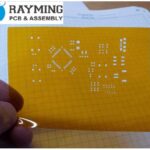
The Rayming stencil-mate is a widely used tool in the electronics manufacturing industry for printing solder paste and other materials onto PCBs. Let’s take a closer look at its features and capabilities.
Overview of the Rayming Stencil-Mate
The Rayming stencil-mate is a manual stencil printer designed for small to medium-scale production. It offers a cost-effective solution for printing solder paste and other materials with high accuracy and consistency.
Key Features and Benefits
Some of the key features and benefits of the Rayming stencil-mate include:
- Compact and portable design
- Adjustable printing parameters for optimal results
- Compatible with a wide range of stencil sizes and thicknesses
- Easy to use and maintain
- Affordable compared to automated printing solutions
Printing Process with the Rayming Stencil-Mate
The printing process with the Rayming stencil-mate involves the following steps:
- Aligning the PCB and stencil
- Applying solder paste to the stencil
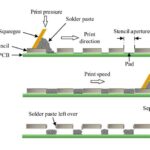
- Spreading the solder paste across the stencil using a squeegee
- Removing the stencil to reveal the printed solder paste on the PCB

Printing Resolution of the Rayming Stencil-Mate
Now, let’s focus on the printing resolution capabilities of the Rayming stencil-mate and the factors that influence the achievable resolution.
Minimum Feature Size
The minimum feature size that can be reliably printed with the Rayming stencil-mate depends on several factors, such as the stencil thickness, aperture size, and solder paste properties. Typically, the Rayming stencil-mate can achieve a minimum feature size of around 0.3mm to 0.4mm (300 to 400 microns) with standard stencils and solder pastes.
Influence of Stencil Thickness on Resolution
Stencil thickness plays a significant role in determining the printing resolution. Thinner stencils allow for finer details and smaller apertures, resulting in higher resolution prints. However, thinner stencils also have limitations in terms of mechanical stability and Solder Paste Volume deposited.
| Stencil Thickness | Typical Minimum Feature Size |
|---|---|
| 100 microns | 0.2mm – 0.25mm |
| 120 microns | 0.25mm – 0.3mm |
| 150 microns | 0.3mm – 0.35mm |
| 200 microns | 0.35mm – 0.4mm |
Impact of Aperture Size and Shape on Resolution
The size and shape of the stencil apertures also influence the printing resolution. Smaller apertures allow for finer details, but they can also present challenges in terms of solder paste release and consistent print quality. Circular apertures tend to provide better solder paste release compared to square or rectangular apertures.
Solder Paste Properties and Resolution
The properties of the solder paste, such as particle size and viscosity, can impact the printing resolution. Solder pastes with smaller particle sizes and lower viscosity are generally better suited for printing fine details and achieving higher resolution.
Optimizing Printing Parameters for Higher Resolution
To achieve the best possible printing resolution with the Rayming stencil-mate, it is essential to optimize the printing parameters, such as squeegee pressure, speed, and angle. Experimenting with different settings and conducting test prints can help determine the optimal parameters for a given stencil and solder paste combination.
Best Practices for High-Resolution Printing
To ensure consistent and reliable high-resolution printing with the Rayming stencil-mate, consider the following best practices:
- Use high-quality stencils with precise aperture dimensions
- Select solder pastes with appropriate particle size and viscosity for fine-pitch printing
- Maintain proper stencil and PCB alignment
- Optimize printing parameters through experimentation and testing
- Regularly clean and maintain the stencil and printing equipment
Case Studies and Real-World Examples
To illustrate the printing resolution capabilities of the Rayming stencil-mate, let’s examine some real-world examples and case studies.
Example 1: Printing 0.4mm Pitch QFN Components
In this example, a manufacturer used the Rayming stencil-mate to print solder paste for 0.4mm pitch QFN (Quad Flat No-lead) components. By using a 150-micron thick stencil and a solder paste with a particle size of 25-45 microns, they successfully achieved reliable printing and soldering of the fine-pitch components.
Example 2: Printing 0.3mm Pitch BGA Components
Another manufacturer demonstrated the capability of the Rayming stencil-mate to print solder paste for 0.3mm pitch BGA (Ball Grid Array) components. Using a 120-micron thick stencil and a solder paste with a particle size of 20-38 microns, they achieved consistent and accurate printing, enabling successful assembly of the high-density BGA Packages.
These examples showcase the Rayming stencil-mate’s ability to print at resolutions suitable for fine-pitch components commonly used in modern electronics manufacturing.
Frequently Asked Questions (FAQ)
-
Q: Can the Rayming stencil-mate print components with a pitch smaller than 0.3mm?
A: While the Rayming stencil-mate has been demonstrated to print components with a pitch as small as 0.3mm, achieving reliable printing below this pitch becomes challenging. It may be possible with specialized stencils and solder pastes, but the results can be inconsistent and require extensive optimization. -
Q: What is the maximum stencil size that can be used with the Rayming stencil-mate?
A: The Rayming stencil-mate can accommodate stencils up to 29 inches x 29 inches (737mm x 737mm), making it suitable for a wide range of PCB sizes and designs. -
Q: Can the Rayming stencil-mate be used with solder pastes other than tin-lead (SnPb)?
A: Yes, the Rayming stencil-mate is compatible with various solder paste alloys, including lead-free options such as SAC (Tin-Silver-Copper) and SnAg (Tin-Silver). However, it’s essential to select a solder paste with appropriate properties for the desired printing resolution. -
Q: How often should the stencil be cleaned when using the Rayming stencil-mate?
A: The frequency of stencil cleaning depends on factors such as the solder paste type, printing volume, and environmental conditions. As a general guideline, it’s recommended to clean the stencil every 4-8 hours of continuous printing or whenever print quality starts to deteriorate. -
Q: Are there any limitations to the type of components that can be printed with the Rayming stencil-mate?
A: The Rayming stencil-mate can print a wide variety of surface mount components, including chip resistors, capacitors, QFNs, BGAs, and more. However, the ability to print specific components depends on their size, pitch, and the available stencil and solder paste options. It’s essential to consult with the manufacturer or a stencil design expert to determine the feasibility of printing specific components.
Conclusion
In conclusion, the Rayming stencil-mate is a versatile and reliable tool for printing solder paste and other materials in electronics manufacturing. With its ability to achieve printing resolutions suitable for components with pitches as small as 0.3mm to 0.4mm, the Rayming stencil-mate enables the production of high-quality PCBs with fine-pitch components.
However, achieving the highest possible printing resolution requires careful consideration of factors such as stencil thickness, aperture size and shape, solder paste properties, and printing parameters. By understanding these factors and following best practices, manufacturers can optimize their printing process and ensure consistent, reliable results.
As the electronics industry continues to push the boundaries of miniaturization and functionality, the Rayming stencil-mate remains a valuable tool for meeting the demanding printing requirements of modern PCB Assembly. With its affordability, ease of use, and proven performance, the Rayming stencil-mate is an excellent choice for manufacturers seeking a cost-effective solution for high-resolution printing.
Leave a Reply