Introduction to PCB Stencils
PCB (Printed Circuit Board) stencils are essential tools in the electronics manufacturing industry. They are used to apply solder paste onto the PCB Pads accurately and consistently, ensuring high-quality solder joints and reliable connections. In this article, we will explore the various aspects of PCB stencils, their importance in the PCB Assembly process, and the advanced services offered by leading PCB stencil manufacturers.
What are PCB Stencils?
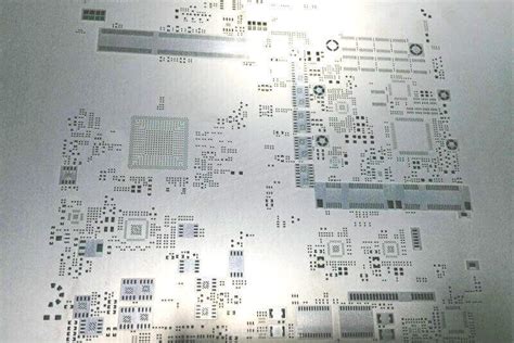
PCB stencils, also known as solder paste stencils, are thin metal sheets with precise openings that correspond to the solder pads on a PCB. These openings allow the solder paste to be deposited onto the pads in a controlled manner, ensuring the right amount of paste is applied for optimal soldering results.
Why are PCB Stencils Important?
PCB stencils play a crucial role in the surface mount technology (SMT) assembly process. They enable the accurate and consistent application of solder paste, which is essential for achieving reliable solder joints between components and the PCB. Without stencils, the solder paste application would be inconsistent, leading to poor Solder Joint Quality and potential device failures.
Types of PCB Stencils
There are several types of PCB stencils available, each with its own characteristics and advantages. Let’s explore the most common types:
Laser-Cut Stencils
Laser-cut stencils are created using high-precision laser cutting technology. The laser beam accurately cuts the openings in the stencil material, resulting in clean and sharp edges. Laser-cut stencils are known for their high accuracy and repeatability, making them suitable for fine-pitch components and high-density PCB designs.
Electroformed Stencils
Electroformed stencils are manufactured using an electroplating process. A thin layer of nickel is deposited onto a photoresist-patterned substrate, creating the stencil openings. Electroformed stencils offer excellent dimensional accuracy and smooth aperture walls, making them ideal for applications requiring high precision and consistency.
Nano-Coated Stencils
Nano-coated stencils feature a special nano-scale coating applied to the stencil surface. This coating helps to reduce solder paste adhesion and improves the release characteristics of the stencil. Nano-coated stencils are particularly useful for printing small apertures and fine-pitch components, as they minimize paste bridging and ensure clean solder paste deposits.

Stencil Materials
PCB stencils can be made from various materials, each with its own properties and advantages. The choice of stencil material depends on factors such as the desired durability, cost, and specific application requirements. Here are the most common stencil materials:
Stainless Steel
Stainless steel is the most widely used material for PCB stencils. It offers excellent durability, strength, and resistance to wear and tear. Stainless steel stencils are suitable for high-volume production and can withstand multiple printing cycles without significant degradation.
Nickel
Nickel stencils are known for their high precision and smooth surface finish. They are often used in applications requiring fine-pitch components and high-density PCB layouts. Nickel stencils are more expensive than stainless steel but offer superior printing quality and longer lifespan.
Polyimide
Polyimide stencils, also known as polymer stencils, are made from a flexible and durable plastic material. They are lightweight and easy to handle, making them suitable for quick prototyping and low-volume production. Polyimide stencils are cost-effective and can be easily cut using laser or die-cutting methods.

Stencil Thickness and Aperture Design
The thickness of a PCB stencil and the design of its apertures play a significant role in determining the quality and consistency of solder paste deposits. Let’s explore these factors in more detail:
Stencil Thickness
The thickness of a PCB stencil directly affects the volume of solder paste deposited onto the PCB pads. Thicker stencils deposit more paste, while thinner stencils deposit less. The choice of stencil thickness depends on factors such as the size of the components, the pitch of the pads, and the desired solder joint profile.
| Component Pitch | Recommended Stencil Thickness |
|---|---|
| > 0.65 mm | 150 – 200 µm |
| 0.5 – 0.65 mm | 120 – 150 µm |
| 0.4 – 0.5 mm | 100 – 120 µm |
| < 0.4 mm | 80 – 100 µm |
Aperture Design
The aperture design of a PCB stencil refers to the shape and size of the openings that allow solder paste to be deposited onto the PCB pads. The aperture design should be optimized to ensure the right amount of paste is deposited and to prevent issues such as paste bridging or insufficient coverage.
Common aperture designs include:
- Square: Simple and commonly used for larger pads
- Circular: Suitable for smaller pads and fine-pitch components
- Rectangular: Used for elongated pads or connectors
- D-Shaped: Combines the benefits of square and circular apertures

Stencil Inspection and Quality Control
To ensure the highest quality and consistency of PCB stencils, manufacturers employ various inspection and quality control measures. These measures help to identify and rectify any defects or inconsistencies in the stencils before they are used in the PCB assembly process.
Automated Optical Inspection (AOI)
AOI systems use high-resolution cameras and advanced image processing algorithms to inspect PCB stencils for defects such as aperture blockages, damage, or dimensional inaccuracies. AOI enables rapid and accurate inspection of stencils, reducing the risk of defective stencils being used in production.
3D Scanning and Measurement
3D scanning and measurement technologies, such as laser scanners or white light interferometry, are used to create detailed 3D models of PCB stencils. These models allow for precise measurement of aperture dimensions, stencil thickness, and surface flatness. By comparing the scanned data with the original design, manufacturers can verify the accuracy and consistency of the stencils.
Statistical Process Control (SPC)
SPC is a quality control methodology that involves collecting and analyzing process data to monitor and control the manufacturing process. By tracking key parameters such as aperture dimensions, stencil thickness, and print quality, manufacturers can identify trends and variations in the process and take corrective actions to maintain consistent stencil quality.
Advanced PCB Stencil Services
Leading PCB stencil manufacturers offer a range of advanced services to cater to the diverse needs of their customers. These services aim to provide high-quality stencils, fast turnaround times, and expert support throughout the PCB assembly process.
Custom Stencil Design
Many stencil manufacturers offer custom stencil design services to optimize the stencil layout for specific PCB designs. This involves working closely with customers to understand their requirements, analyzing the PCB layout, and recommending the best stencil specifications, such as thickness, aperture design, and material choice.
Quick-Turn Production
In today’s fast-paced electronics industry, quick turnaround times are crucial. Many stencil manufacturers offer expedited production services, allowing customers to receive their stencils within a matter of days. This is particularly useful for prototyping, urgent production runs, or time-sensitive projects.
Stencil Maintenance and Repair
To extend the lifespan of PCB stencils and maintain their performance, regular maintenance and repair services are essential. Stencil manufacturers offer cleaning, inspection, and repair services to remove solder paste residue, fix damaged apertures, and ensure the stencils remain in optimal condition for reliable printing results.
Technical Support and Consulting
Stencil manufacturers often provide technical support and consulting services to assist customers in optimizing their PCB assembly processes. This includes guidance on stencil selection, printing parameters, solder paste specifications, and troubleshooting support. By leveraging the expertise of stencil professionals, customers can improve their assembly yields, reduce defects, and achieve better overall product quality.
Frequently Asked Questions (FAQ)
-
Q: What is the typical lifespan of a PCB stencil?
A: The lifespan of a PCB stencil depends on various factors, such as the material, thickness, and usage frequency. On average, a well-maintained stainless steel stencil can last for 20,000 to 50,000 print cycles, while a nickel stencil can last even longer, up to 100,000 print cycles. -
Q: How often should I clean my PCB stencil?
A: It is recommended to clean your PCB stencil after every print cycle to remove solder paste residue and prevent aperture clogging. Regular cleaning helps to maintain print quality and extend the stencil’s lifespan. For high-volume production, automated stencil cleaning systems can be used to streamline the cleaning process. -
Q: Can I reuse a damaged PCB stencil?
A: It depends on the extent of the damage. Minor damage, such as small dents or scratches, can often be repaired by a professional stencil repair service. However, if the damage is severe, such as large tears or deformed apertures, it is advisable to replace the stencil to ensure the best printing results. -
Q: How do I choose the right stencil thickness for my PCB design?
A: The choice of stencil thickness depends on factors such as the component pitch, pad size, and desired solder joint profile. As a general guideline, thinner stencils (80-100 µm) are suitable for fine-pitch components, while thicker stencils (150-200 µm) are used for larger components and pads. It is recommended to consult with your stencil manufacturer for specific guidance based on your PCB design. -
Q: What is the difference between laser-cut and electroformed stencils?
A: Laser-cut stencils are created using high-precision laser cutting technology, resulting in clean and sharp aperture edges. They are suitable for a wide range of PCB designs and offer good durability. Electroformed stencils, on the other hand, are made using an electroplating process, resulting in smooth aperture walls and excellent dimensional accuracy. They are ideal for high-precision applications and fine-pitch components but are generally more expensive than laser-cut stencils.
Conclusion
PCB stencils play a critical role in ensuring the quality and reliability of solder paste application in the PCB assembly process. By understanding the different types of stencils, materials, and design considerations, manufacturers can select the most suitable stencil solutions for their specific applications.
Advanced PCB stencil services, such as custom design, quick-turn production, maintenance, and technical support, provide customers with the expertise and flexibility needed to optimize their assembly processes and achieve the best possible results.
As the electronics industry continues to evolve, with increasingly complex PCB designs and smaller component sizes, the importance of high-quality PCB stencils will only grow. By partnering with experienced and reliable stencil manufacturers, companies can ensure they have access to the latest technologies, materials, and support to meet the ever-changing demands of the market.


Leave a Reply