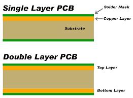
Composition of the Outer PCB Layer
The outer layer of a PCB typically consists of the following components:
-
Copper foil: A thin layer of copper that is laminated onto the base material (substrate) of the PCB. The copper foil is used to create conductive traces, pads, and planes on the outer layer.
-
Solder mask: A protective coating applied over the copper traces and pads, leaving only the exposed areas where components will be soldered. The solder mask is usually green in color but can also be found in other colors, such as red, blue, or black.
-
Silkscreen: A printed layer of text and symbols on top of the solder mask that provides identification and orientation information for the PCB, such as component designators, logos, and assembly instructions.
-
Surface finish: A metallic coating applied to the exposed copper areas to prevent oxidation and enhance solderability. Common surface finishes include Hot Air Solder Leveling (HASL), Organic Solderability Preservative (OSP), Electroless Nickel Immersion Gold (ENIG), and Immersion Silver (IAg).
Functions of the Outer PCB Layer
The outer PCB layer serves several essential functions:
-
Protection: The solder mask and surface finish protect the copper traces and pads from oxidation, corrosion, and mechanical damage, ensuring the long-term reliability of the PCB.
-
Insulation: The solder mask acts as an insulating layer, preventing short circuits between adjacent traces and pads.
-
Solderability: The exposed copper areas with the surface finish provide a solderable surface for component attachment during the assembly process.
-
Identification: The silkscreen layer provides vital information for PCB Assembly, debugging, and maintenance, such as component placement, polarity indicators, and test points.
-
Aesthetics: The outer layer contributes to the overall appearance of the PCB, with the solder mask color and silkscreen design creating a professional and branded look.

Manufacturing Process of the Outer PCB Layer
The manufacturing process of the outer PCB layer involves several steps:
-
Copper foil lamination: The copper foil is laminated onto the base material using heat and pressure, creating a strong bond between the layers.
-
Photolithography: A photoresist layer is applied to the copper foil and then exposed to UV light through a patterned photomask. The exposed areas of the photoresist are developed and removed, leaving the desired copper pattern.
-
Etching: The exposed copper areas are chemically etched away, leaving only the copper traces and pads protected by the photoresist.
-
Solder mask application: The solder mask is applied over the entire outer layer, typically using a silkscreen printing process. The solder mask is then cured using UV light.
-
Silkscreen printing: The silkscreen layer is printed on top of the solder mask using a similar silkscreen printing process, with ink that is cured using heat or UV light.
-
Surface finish application: The exposed copper areas are coated with the chosen surface finish using various methods, such as immersion, electroplating, or hot air solder leveling.

Design Considerations for the Outer PCB Layer
When designing the outer PCB layer, several factors must be considered to ensure optimal performance and manufacturability:
-
Trace width and spacing: The width and spacing of the copper traces must be carefully designed to maintain signal integrity, minimize crosstalk, and ensure manufacturability. The specific requirements depend on the signal frequency, current carrying capacity, and PCB Fabrication capabilities.
-
Pad size and shape: The size and shape of the component pads must be designed to accommodate the specific package types and ensure reliable soldering. Factors such as the solder mask opening, surface finish, and thermal requirements must also be considered.
-
Solder mask design: The solder mask opening should be slightly larger than the copper pad to allow for proper solder wetting and prevent solder bridging. The solder mask also requires adequate clearance around traces and pads to prevent insulation issues.
-
Silkscreen legibility: The silkscreen text and symbols must be legible and properly aligned with the corresponding components and features. The font size, line width, and spacing should be chosen based on the PCB fabrication capabilities and the minimum readable size for the assembler.
-
Surface Finish Selection: The choice of surface finish depends on various factors, such as the component types, soldering process, shelf life, and cost. Each surface finish has its advantages and disadvantages, which must be carefully considered based on the specific application requirements.
-
Design for manufacturing (DFM): The outer PCB layer design must adhere to the DFM guidelines provided by the PCB fabricator to ensure high yields and minimize manufacturing defects. This includes factors such as minimum feature sizes, copper-to-edge clearance, and soldermask dam size.

Advancements in Outer PCB Layer Technology
As PCB technology continues to evolve, several advancements have been made in the outer layer design and manufacturing process:
-
High-density interconnect (HDI): HDI PCBs feature finer trace widths and smaller pad sizes, enabling higher component density and improved signal integrity. Advanced manufacturing techniques, such as laser drilling and sequential build-up, are used to create HDI outer layers.
-
Embedded components: Some advanced PCBs feature embedded components, such as capacitors and resistors, within the outer layer. This technique saves space and improves performance by reducing the distance between components and the PCB surface.
-
3D printing: Additive manufacturing techniques, such as 3D printing, are being explored for creating PCB outer layers with complex geometries and unique features. This technology enables rapid prototyping and customization of PCBs.
-
Flexible and stretchable PCBs: Flexible and stretchable PCBs are gaining popularity in wearable electronics and IoT applications. These PCBs feature outer layers made of flexible materials, such as polyimide or thermoplastic polyurethane (TPU), that can bend and stretch without damaging the conductive traces.
-
Environmentally friendly materials: There is a growing trend towards using environmentally friendly materials in PCB manufacturing, such as lead-free solders, Halogen-Free Solder masks, and biodegradable substrate materials. These materials reduce the environmental impact of PCBs and comply with international regulations, such as RoHS and REACH.
FAQ
1. What is the purpose of the solder mask on the outer PCB layer?
The solder mask serves two main purposes on the outer PCB layer:
-
It acts as an insulating layer, preventing short circuits between adjacent copper traces and pads.
-
It provides protection for the copper features from oxidation, corrosion, and mechanical damage, ensuring the long-term reliability of the PCB.
2. How does the choice of surface finish affect the outer PCB layer?
The choice of surface finish on the outer PCB layer affects several aspects:
-
Solderability: Different surface finishes have varying levels of solderability, which can affect the ease and reliability of the component attachment process.
-
Shelf life: Some surface finishes, such as OSP, have a limited shelf life and may degrade over time, while others, like ENIG, offer extended shelf life.
-
Cost: The cost of applying different surface finishes varies, with some options, like ENIG, being more expensive than others, such as HASL.
-
Compatibility: The surface finish must be compatible with the components and soldering process used in the PCB assembly to ensure reliable connections.
3. What is the significance of the silkscreen layer on the outer PCB layer?
The silkscreen layer on the outer PCB layer is essential for several reasons:
-
It provides vital information for PCB assembly, such as component placement, orientation, and polarity indicators.
-
It helps in debugging and maintenance by providing test points, labels, and other relevant information.
-
It enhances the aesthetic appearance of the PCB, allowing for branding, logos, and other design elements.
4. What are some common design challenges faced when creating the outer PCB layer?
Some common design challenges encountered when creating the outer PCB layer include:
-
Maintaining proper trace width and spacing to ensure signal integrity and manufacturability.
-
Designing component pads with the appropriate size, shape, and solder mask opening for reliable soldering.
-
Ensuring the legibility and alignment of the silkscreen layer while adhering to minimum font sizes and spacing requirements.
-
Selecting the appropriate surface finish based on the specific application requirements, such as component compatibility, shelf life, and cost.
-
Adhering to the design for manufacturing (DFM) guidelines provided by the PCB fabricator to minimize manufacturing defects and improve yields.
5. How can the outer PCB layer design contribute to the overall performance of the PCB?
The outer PCB layer design can contribute to the overall performance of the PCB in several ways:
-
By ensuring proper trace width and spacing, the outer layer can maintain signal integrity, minimize crosstalk, and reduce electromagnetic interference (EMI).
-
The choice of surface finish can affect the solderability and long-term reliability of the components attached to the outer layer.
-
A well-designed solder mask and silkscreen layer can improve the manufacturing process and reduce assembly errors, leading to higher quality and reliability of the final product.
-
By considering the specific application requirements and selecting the appropriate materials and features, the outer layer design can optimize the PCB’s performance in terms of signal quality, power distribution, and mechanical stability.
Conclusion
The outer layer of a PCB is a critical component that serves multiple functions, including protection, insulation, solderability, identification, and aesthetics. The composition of the outer layer includes copper foil, solder mask, silkscreen, and surface finish, each contributing to the overall performance and reliability of the PCB.
The manufacturing process of the outer PCB layer involves several steps, from copper foil lamination to surface finish application, requiring precise control and adherence to design guidelines. When designing the outer layer, engineers must consider factors such as trace width and spacing, pad size and shape, solder mask design, silkscreen legibility, surface finish selection, and design for manufacturing.
Advancements in outer PCB layer technology, such as high-density interconnects, embedded components, 3D printing, flexible and stretchable materials, and environmentally friendly solutions, are driving innovation and expanding the applications of PCBs in various industries.
By understanding the importance of the outer PCB layer and considering the design challenges and best practices, engineers can create high-quality, reliable, and performance-optimized PCBs for a wide range of applications.
Here is a summary table of the key aspects of the outer PCB layer:
| Aspect | Description |
|---|---|
| Composition | Copper foil, solder mask, silkscreen, surface finish |
| Functions | Protection, insulation, solderability, identification, aesthetics |
| Manufacturing Process | Copper foil lamination, photolithography, etching, solder mask application, silkscreen printing, surface finish application |
| Design Considerations | Trace width and spacing, pad size and shape, solder mask design, silkscreen legibility, surface finish selection, design for manufacturing |
| Advancements | High-density interconnect, embedded components, 3D printing, flexible and stretchable materials, environmentally friendly solutions |
By considering these aspects and staying updated with the latest advancements in outer PCB layer technology, engineers can design and manufacture high-quality PCBs that meet the ever-increasing demands of modern electronic devices.


Leave a Reply