Introduction to IMS-PCB-vlak technology
In recent years, the lighting industry has seen a significant shift towards energy-efficient and environmentally friendly solutions. One such innovation is the use of Insulated Metal Substrate (IMS) Printed Circuit Boards (PCBs) in the production of ambient lighting, particularly in the form of “vlak” or flat panel lights. This article will delve into the intricacies of IMS-PCB-vlak technology, its advantages, applications, and future prospects.
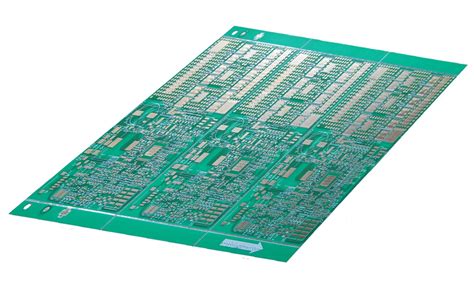
What is an IMS PCB?
An Insulated Metal Substrate (IMS) PCB is a specialized type of printed circuit board that consists of a metal base layer, typically aluminum, which is coated with a thin layer of dielectric material. The dielectric layer provides electrical insulation between the metal substrate and the copper circuit layer. IMS PCBs are known for their excellent thermal management properties, as the metal substrate helps dissipate heat more efficiently than traditional FR-4 PCBs.
Advantages of IMS PCBs in lighting applications
IMS PCBs offer several advantages when used in lighting applications, particularly in LED-based systems:
-
Enhanced thermal management: The metal substrate of an IMS PCB acts as a heat sink, allowing for better heat dissipation from the LED components. This results in improved LED performance, longer lifespan, and reduced risk of thermal damage.
-
Increased power density: IMS PCBs can handle higher power densities compared to traditional PCBs, enabling the design of more compact and efficient lighting systems.
-
Improved reliability: The enhanced thermal management properties of IMS PCBs contribute to the overall reliability of the lighting system, reducing the risk of component failure due to thermal stress.
-
Cost-effectiveness: IMS PCBs can be a cost-effective solution for lighting applications, as they eliminate the need for additional heat sinks and thermal management components.
The concept of “vlak” ambient lighting
“Vlak” is a Dutch term meaning “flat” or “level.” In the context of ambient lighting, “vlak” refers to flat panel lights that provide even illumination across a wide area. These flat panel lights are designed to be slim, unobtrusive, and energy-efficient, making them ideal for a variety of indoor and outdoor applications.
Benefits of “vlak” ambient lighting
“Vlak” ambient lighting offers several benefits, including:
-
Uniform illumination: Flat panel lights provide even illumination across the entire surface, eliminating hot spots and shadows.
-
Slim profile: The slim design of “vlak” lights allows for easy integration into various architectural and design elements.
-
Energy efficiency: “Vlak” lights are typically LED-based, which means they consume less energy compared to traditional lighting solutions.
-
Versatility: Flat panel lights can be used in a wide range of applications, from residential and commercial spaces to industrial and outdoor environments.
Applications of “vlak” ambient lighting
“Vlak” ambient lighting finds use in numerous applications, such as:
- Office and workspace lighting
- Retail and hospitality lighting
- Architectural and decorative lighting
- Outdoor and landscape lighting
- Automotive and transportation lighting

IMS PCBs as the foundation of “vlak” ambient lighting
IMS PCBs play a crucial role in the development and production of “vlak” ambient lights. The unique properties of IMS PCBs make them particularly well-suited for flat panel lighting applications.
Thermal management in “vlak” lights
One of the key challenges in designing flat panel lights is ensuring proper thermal management. As LEDs generate heat during operation, it is essential to dissipate this heat effectively to maintain optimal performance and longevity. IMS PCBs, with their metal substrate acting as a built-in heat sink, provide an ideal solution for thermal management in “vlak” lights.
The metal substrate, usually aluminum, efficiently conducts heat away from the LED components, preventing thermal buildup and ensuring stable operation. This integrated thermal management solution eliminates the need for additional heat sinks, resulting in a more compact and streamlined design.
Designing IMS PCBs for “vlak” lights
When designing IMS PCBs for “vlak” ambient lighting, several factors must be considered to ensure optimal performance and reliability:
-
Dielectric layer thickness: The thickness of the dielectric layer between the metal substrate and the copper circuit layer should be carefully selected to provide adequate electrical insulation while minimizing Thermal Resistance.
-
Copper thickness: The thickness of the copper circuit layer should be chosen based on the current carrying requirements of the LED components, ensuring minimal voltage drop and efficient power distribution.
-
Thermal vias: Thermal vias, which are conductive paths through the dielectric layer, can be incorporated into the IMS PCB design to further enhance heat dissipation from the LED components to the metal substrate.
-
Component placement: The placement of LED components on the IMS PCB should be optimized to ensure even heat distribution and minimize thermal stress on individual components.
Manufacturing process for IMS PCBs
The manufacturing process for IMS PCBs differs from that of traditional FR-4 PCBs due to the presence of the metal substrate. The main steps involved in the production of IMS PCBs include:
-
Substrate preparation: The metal substrate, typically aluminum, is cleaned and treated to ensure proper adhesion of the dielectric layer.
-
Dielectric layer application: The dielectric layer, which can be a polymer or a ceramic material, is applied to the metal substrate using techniques such as lamination, spraying, or screen printing.
-
Copper foil lamination: A copper foil is laminated onto the dielectric layer using heat and pressure.
-
Circuit patterning: The desired circuit pattern is transferred onto the copper layer using photolithography and etching processes.
-
Component assembly: LED components and other electronic components are soldered onto the IMS PCB using standard SMT (Surface Mount Technology) processes.
-
Quality control: The assembled IMS PCB undergoes various quality control checks to ensure proper functionality, reliability, and adherence to specifications.

Future trends and developments in IMS-PCB-vlak technology
As the demand for energy-efficient and high-performance lighting solutions continues to grow, IMS-PCB-vlak technology is poised for further advancements and innovations.
Advancements in materials and manufacturing processes
Researchers and manufacturers are continually exploring new materials and manufacturing processes to improve the performance and cost-effectiveness of IMS PCBs. Some of the recent developments include:
-
Nanoceramic dielectric materials: Nanoceramic materials offer higher thermal conductivity and lower thermal resistance compared to traditional polymer dielectrics, enabling even better thermal management in IMS PCBs.
-
3D printing of IMS PCBs: Additive manufacturing techniques, such as 3D printing, are being investigated for the production of IMS PCBs, potentially enabling more complex geometries and customized designs.
-
Embedded components: The integration of electronic components directly into the IMS PCB substrate is an emerging trend that can lead to more compact and efficient designs.
Integration of smart features and IoT capabilities
As the lighting industry embraces the Internet of Things (IoT) and smart technologies, “vlak” ambient lights are expected to incorporate advanced features such as:
-
Wireless connectivity: Integration of wireless Communication Protocols, such as Wi-Fi, Bluetooth, or Zigbee, will enable remote control and monitoring of “vlak” lights through smartphones, tablets, or other connected devices.
-
Sensor integration: Incorporation of sensors, such as occupancy sensors, dayLight Sensors, or color sensors, will allow “vlak” lights to adapt to the environment and optimize energy consumption.
-
Data analytics: Connected “vlak” lights can generate valuable data on energy usage, occupancy patterns, and other metrics, enabling data-driven decision making and energy optimization strategies.

FAQs
-
Q: What is the main advantage of using IMS PCBs in “vlak” ambient lighting?
A: The main advantage of using IMS PCBs in “vlak” ambient lighting is their excellent thermal management properties. The metal substrate of an IMS PCB acts as a built-in heat sink, efficiently dissipating heat from the LED components and ensuring optimal performance and longevity. -
Q: Can IMS PCBs be used in outdoor lighting applications?
A: Yes, IMS PCBs can be used in outdoor lighting applications. The enhanced thermal management and high power handling capabilities of IMS PCBs make them suitable for a wide range of outdoor lighting applications, such as street lighting, landscape lighting, and architectural lighting. -
Q: How does the manufacturing process for IMS PCBs differ from that of traditional FR-4 PCBs?
A: The manufacturing process for IMS PCBs differs from that of traditional FR-4 PCBs in several ways. IMS PCBs require additional steps such as substrate preparation, dielectric layer application, and copper foil lamination, which are not present in the production of FR-4 PCBs. Additionally, the choice of materials and processing parameters must be optimized for the specific requirements of IMS PCBs. -
Q: What are some of the future trends in IMS-PCB-vlak technology?
A: Some of the future trends in IMS-PCB-vlak technology include the development of advanced materials (such as nanoceramic dielectrics), innovative manufacturing processes (like 3D printing), and the integration of smart features and IoT capabilities. These advancements aim to further improve the performance, efficiency, and functionality of “vlak” ambient lighting solutions. -
Q: Are “vlak” ambient lights more energy-efficient than traditional lighting solutions?
A: Yes, “vlak” ambient lights are typically more energy-efficient than traditional lighting solutions. This is because “vlak” lights are usually LED-based, which consume less energy compared to incandescent or fluorescent lamps. Additionally, the use of IMS PCBs in “vlak” lights enables better thermal management, which further contributes to energy efficiency by ensuring optimal LED performance and longevity.
Conclusion
IMS-PCB-vlak technology represents a significant advancement in the field of ambient lighting, offering a range of benefits including improved thermal management, increased power density, and enhanced energy efficiency. By leveraging the unique properties of IMS PCBs, “vlak” ambient lights can provide uniform illumination, slim profiles, and versatile applications across various sectors.
As the lighting industry continues to evolve, IMS-PCB-vlak technology is expected to play a crucial role in shaping the future of ambient lighting. With ongoing advancements in materials, manufacturing processes, and the integration of smart features, “vlak” lights are poised to become even more efficient, adaptable, and intelligent.
By embracing IMS-PCB-vlak technology, lighting manufacturers, designers, and end-users can unlock new possibilities in creating sustainable, high-performance, and visually appealing ambient lighting solutions. As the world moves towards a more energy-conscious and connected future, IMS-PCB-vlak technology will undoubtedly continue to light the way forward.


Leave a Reply