What is Solder Escape?
Solder escape, also known as solder wicking, is a common issue in Electronic Assembly where molten solder flows or “wicks” away from the intended joint, along the component lead or PCB trace. This can result in insufficient solder at the joint, leading to poor electrical connections, reduced mechanical strength, and potential reliability issues.
Solder escape is particularly problematic during reflow soldering, a process used to attach surface mount components to a printed circuit board (PCB). In reflow soldering, solder paste (a mixture of powdered solder and flux) is applied to the PCB pads, components are placed, and the assembly is heated in a reflow oven to melt the solder and form the joints.
Causes of Solder Escape
Several factors can contribute to solder escape during reflow:
Excessive Solder Paste
Applying too much solder paste can cause the excess molten solder to flow away from the joint along the component lead or PCB trace. This is especially true for small components with fine pitch leads.
Incorrect Solder Paste Viscosity
Solder paste viscosity, or thickness, plays a crucial role in preventing solder escape. If the paste is too thin, it may flow too easily and wick away from the joint. On the other hand, if it’s too thick, it may not flow properly and result in poor joint formation.
Improper Reflow Profile
The reflow temperature profile must be optimized for the specific solder paste and PCB design. If the peak temperature is too high or the time above liquidus (TAL) is too long, the molten solder may become excessively fluid and prone to escape.
Poor Wetting
Wetting refers to the ability of molten solder to adhere to and spread on a surface. Poor wetting can be caused by contaminants, oxidation, or incompatible surface finishes, leading to solder escape as the molten solder seeks a more wettable surface.
Inadequate Pad Design
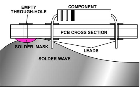
PCB pad size and shape can influence solder escape. If the pads are too small or have insufficient solder mask clearance, the molten solder may wick away along the trace. Properly designed pads with adequate solder mask dams can help contain the solder.

Tips for Preventing Solder Escape
To minimize the risk of solder escape during reflow, consider the following tips:
1. Optimize Solder Paste Application
- Use a solder paste with the appropriate viscosity for your application. Consult the paste manufacturer’s recommendations and conduct trials to determine the optimal viscosity.
- Ensure the solder paste is evenly applied to the PCB pads using a stencil with the correct aperture size and shape. Avoid excessive paste deposition.
- Regularly inspect and maintain your solder paste printing equipment to ensure consistent paste application.
2. Control Reflow Profile
- Develop a reflow profile tailored to your specific solder paste and PCB design. Follow the paste manufacturer’s recommended profile as a starting point and fine-tune as needed.
- Monitor the peak temperature and time above liquidus (TAL) to avoid overheating the solder. Excessive temperature or prolonged TAL can increase solder fluidity and escape.
- Use a reflow oven with good temperature control and uniformity to ensure consistent heating across the PCB.
3. Ensure Proper Wetting
- Specify PCB Finishes that promote good solder wetting, such as immersion silver (ImAg), electroless nickel immersion gold (ENIG), or organic solderability preservative (OSP).
- Clean the PCB and components thoroughly before assembly to remove contaminants that may hinder wetting.
- Use a nitrogen atmosphere in the reflow oven to minimize oxidation and improve wetting.
4. Optimize Pad Design
- Design PCB pads with adequate size and shape to accommodate the solder volume and component geometry. Follow IPC guidelines and component manufacturer recommendations.
- Incorporate solder mask dams around pads to help contain the molten solder and prevent escape along the traces.
- Avoid excessively long or narrow traces that may encourage solder wicking.
5. Monitor and Inspect
- Implement a robust process monitoring and control system to ensure consistent solder paste application, component placement, and reflow conditions.
- Regularly inspect reflowed assemblies for signs of solder escape using visual inspection, automated optical inspection (AOI), or X-ray inspection for hidden joints.
- Analyze defects and process data to identify trends and implement corrective actions as needed.

Examples and Case Studies
Example 1: Fine Pitch QFN Solder Escape
A manufacturer was experiencing solder escape issues on fine pitch quad flat no-lead (QFN) packages. The escape occurred along the component leads, resulting in insufficient solder joints and poor electrical connections.
Upon investigation, it was found that the solder paste viscosity was too low, allowing the molten solder to flow too easily. Additionally, the reflow profile had an excessive peak temperature, further increasing solder fluidity.
To resolve the issue, the manufacturer switched to a higher viscosity solder paste and optimized the reflow profile to reduce the peak temperature. They also improved the PCB pad design by adding solder mask dams to contain the solder. These changes successfully eliminated the solder escape problem.
Example 2: BGA Solder Escape
An assembler encountered solder escape on ball grid array (BGA) packages during reflow. The solder was wicking away from the BGA balls along the PCB traces, causing open circuits and poor joint strength.
Analysis revealed that the root cause was poor wetting due to contamination on the PCB surface. The assembler had not adequately cleaned the PCBs before solder paste application, leaving residues that hindered solder adhesion.
To solve the problem, the assembler implemented a more thorough PCB Cleaning process using an appropriate cleaning agent and method. They also started using a nitrogen atmosphere in the reflow oven to minimize oxidation and enhance wetting. These improvements successfully resolved the BGA solder escape issue.

Frequently Asked Questions (FAQ)
1. What is solder paste viscosity, and why is it important?
Solder paste viscosity refers to the thickness or resistance to flow of the paste. It is important because it affects how easily the molten solder can flow and spread during reflow. If the viscosity is too low, the solder may flow too readily and escape from the intended joint. If it’s too high, the solder may not flow properly and result in poor joint formation. Selecting the appropriate viscosity for the application is crucial for preventing solder escape and ensuring good joint quality.
2. How can I determine the optimal reflow profile for my solder paste and PCB?
To determine the optimal reflow profile, start by consulting the solder paste manufacturer’s recommended profile. This will provide a baseline for the key parameters such as peak temperature, time above liquidus (TAL), ramp rates, and soak times. Next, consider your specific PCB design, component types, and thermal mass. Conduct reflow profile trials and analyze the results, looking for signs of solder escape, poor wetting, or other defects. Fine-tune the profile parameters until you achieve the desired joint quality and reliability. It’s also important to regularly monitor and verify the reflow profile to ensure consistency.
3. What are solder mask dams, and how do they help prevent solder escape?
Solder mask dams are raised features of solder mask material placed aRound PCB pads. They act as barriers to contain the molten solder and prevent it from flowing away along the traces. By effectively creating a “dam” around the pad, solder mask dams help maintain the solder volume at the intended joint and minimize the risk of solder escape. When designing PCBs, it’s important to include appropriate solder mask dams, especially for fine pitch components or areas prone to solder escape.
4. Can solder escape be detected by visual inspection?
In many cases, solder escape can be detected by visual inspection of the reflowed assembly. Escaped solder often appears as thin, elongated filaments extending from the joint along the component lead or PCB trace. However, visual inspection may not always be sufficient, particularly for hidden or obscured joints such as those under BGA packages. In these cases, automated optical inspection (AOI) or X-ray inspection may be necessary to detect solder escape and verify joint quality.
5. How can process monitoring and control help prevent solder escape?
Process monitoring and control play a vital role in preventing solder escape and ensuring consistent assembly quality. By continuously monitoring key process parameters such as solder paste application, component placement accuracy, and reflow temperature profiles, potential issues can be identified and corrected before they lead to defects like solder escape. Implementing statistical process control (SPC) techniques, setting appropriate control limits, and regularly analyzing process data helps maintain the process within acceptable ranges and minimize the risk of solder escape. Additionally, regular equipment maintenance, calibration, and operator training contribute to a robust and stable assembly process.
Conclusion
Solder escape is a common challenge in electronic assembly that can lead to poor joint quality, reduced reliability, and costly rework. By understanding the causes of solder escape and implementing best practices for prevention, manufacturers can significantly reduce the occurrence of this defect.
Key strategies for avoiding solder escape include optimizing solder paste application, controlling the reflow profile, ensuring proper wetting, and designing PCBs with appropriate pad geometry and solder mask dams. Regular process monitoring, inspection, and continuous improvement are also essential for maintaining consistent assembly quality.
By following these tips and tricks, electronics manufacturers can minimize solder escape issues, improve first-pass yield, and produce high-quality, reliable products. As with any complex manufacturing process, it’s important to stay informed about the latest industry guidelines, materials, and technologies to stay ahead of the curve in preventing solder escape and other assembly defects.


Leave a Reply