What is Multilayer PCB Pressing?
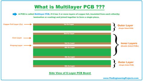
Multilayer PCB pressing is a critical step in the manufacturing process of printed circuit boards (PCBs) that have more than two conductive copper layers. The pressing process involves stacking and laminating multiple layers of copper and insulating material together under high temperature and pressure to create a single, solid board.
The main purpose of multilayer PCB pressing is to ensure the mechanical and electrical integrity of the final board. By bonding the layers together tightly, the pressing process eliminates any air gaps or voids that could compromise the performance and reliability of the PCB.
Why Use Multilayer PCBs?
Multilayer PCBs offer several advantages over single or double-sided boards:
-
Increased Density: Multilayer PCBs allow for a higher density of components and interconnections, enabling more complex and compact designs.
-
Improved Signal Integrity: By using dedicated power and ground planes and shorter signal paths, multilayer PCBs can minimize electromagnetic interference (EMI) and signal crosstalk.
-
Enhanced Thermal Management: Inner layers can be used for heat dissipation, helping to prevent overheating of components.
-
Better Mechanical Strength: The laminated structure of multilayer PCBs provides greater rigidity and durability compared to thinner boards.
The Multilayer PCB Pressing Process
The pressing process for multilayer PCBs typically involves the following steps:
1. Layer Preparation
Before pressing, each layer of the PCB is prepared separately. This includes:
- Etching: The copper layers are selectively etched to create the desired circuit patterns.
- Drilling: Holes are drilled through the layers to accommodate vias and component leads.
- Laminate Cutting: The insulating laminate material is cut to the required size for each layer.
2. Layer Stacking
The prepared layers are stacked in the proper sequence, with the copper sides facing each other. The stack typically includes:
- Core Layers: Pre-etched and drilled double-sided boards that form the backbone of the multilayer PCB.
- Prepreg Layers: Thin sheets of pre-impregnated fiberglass that act as insulation between the copper layers.
- Copper Foils: Additional copper foils are placed on the top and bottom of the stack to create the outer layers of the PCB.
The stacking order is crucial to ensure the correct alignment and connectivity of the layers.
3. Lamination
The stacked layers are placed in a lamination press, which applies high temperature and pressure to bond them together. The typical lamination parameters for multilayer PCBs are:
| Parameter | Value |
|---|---|
| Temperature | 180-200°C |
| Pressure | 250-400 psi |
| Time | 1-2 hours |
During lamination, the prepreg layers melt and flow, filling any gaps between the layers and creating a solid, homogeneous board.
4. Cooling and Finishing
After lamination, the pressed board is cooled gradually to room temperature to prevent warping or delamination. The board then undergoes final finishing steps, such as:
- Drilling: Additional holes are drilled for component mounting and via connections.
- Plating: The drilled holes are plated with copper to create electrical connections between layers.
- Solder Mask Application: A protective solder mask is applied to the outer layers to prevent short circuits and improve solderability.
- Surface Finish: A surface finish, such as HASL, ENIG, or OSP, is applied to the exposed copper areas to protect them from oxidation and enhance solderability.

Factors Affecting Multilayer PCB Pressing Quality
Several factors can impact the quality and reliability of the pressing process:
1. Material Selection
Choosing the right materials is essential for successful multilayer PCB pressing. The key materials to consider are:
- Laminate: The base material for the core layers, typically FR-4 or high-frequency laminates like Rogers or Isola.
- Prepreg: The type and thickness of the prepreg should be selected based on the desired layer spacing and dielectric properties.
- Copper Foil: The copper foil thickness and type (electrodeposited or rolled) affect the electrical and thermal performance of the PCB.
2. Layer Alignment
Proper alignment of the layers during stacking is critical to ensure the correct registration of vias, pads, and traces. Misalignment can lead to open or short circuits, compromising the functionality of the PCB.
To achieve accurate alignment, various methods are used, such as:
- Tooling Holes: Precise holes drilled in each layer that match corresponding pins in the stacking fixture.
- Optical Alignment: Using camera systems to align the layers based on fiducial marks or features.
3. Pressing Parameters
The temperature, pressure, and duration of the lamination process must be carefully controlled to achieve optimal bonding and avoid defects. Insufficient or excessive pressing can result in issues like:
- Delamination: Separation of the layers due to poor bonding.
- Warping: Distortion of the board due to uneven heating or cooling.
- Resin Starvation: Insufficient flow of prepreg resin, leading to voids or poor insulation between layers.
Proper calibration and monitoring of the lamination press are essential to maintain consistent pressing parameters.
4. Handling and Storage
Multilayer PCBs are sensitive to moisture, temperature, and mechanical stress during handling and storage. Improper handling can lead to defects like:
- Contamination: Dirt, oils, or other contaminants on the layers can interfere with bonding and cause defects.
- Mechanical Damage: Scratches, dents, or bends in the layers can cause misalignment or poor lamination.
- Moisture Absorption: Exposure to high humidity can cause the laminate and prepreg to absorb moisture, leading to delamination or blistering during pressing.
To minimize these issues, multilayer PCBs should be handled in a clean, controlled environment and stored in moisture-barrier bags with desiccants when not in use.
Quality Control and Testing
To ensure the quality and reliability of multilayer PCBs, various inspections and tests are performed throughout the manufacturing process, including:
-
Visual Inspection: Manual or automated inspection of the layers and finished board for defects like misalignment, contamination, or damage.
-
Electrical Testing: Continuity and isolation testing to verify the correct connections and insulation between layers and circuits.
-
Microsectioning: Cross-sectional analysis of the pressed board to check for proper layer bonding, via formation, and thickness uniformity.
-
Thermal Stress Testing: Subjecting the board to temperature cycling or thermal shock to evaluate its resistance to thermal expansion and contraction.
By implementing strict quality control measures and testing procedures, manufacturers can identify and address any issues early in the production process, ensuring the delivery of high-quality multilayer PCBs.
Advantages of Professional Multilayer PCB Pressing Services
While some PCB Fabrication facilities may have in-house pressing capabilities, many manufacturers choose to outsource multilayer PCB pressing to specialized service providers. The benefits of using professional pressing services include:
-
Expertise: Pressing service providers have dedicated teams with extensive experience and knowledge in multilayer PCB lamination, ensuring high-quality results.
-
Advanced Equipment: Professional pressing facilities invest in state-of-the-art lamination presses and process control systems to maintain tight tolerances and consistency.
-
Scalability: Outsourcing pressing allows manufacturers to scale their production capacity up or down based on demand, without the need for capital investment in equipment.
-
Cost-effectiveness: By leveraging the economies of scale and efficiency of specialized pressing services, manufacturers can reduce their overall production costs.
-
Quality Assurance: Pressing service providers often have rigorous quality control processes and certifications, such as ISO 9001, ensuring the consistent delivery of high-quality pressed boards.
When selecting a multilayer PCB pressing service, manufacturers should consider factors such as the provider’s experience, equipment capabilities, turnaround time, and quality management systems to ensure a reliable and successful partnership.
Multilayer PCB Pressing FAQ
1. What is the minimum number of layers required for a PCB to be considered “multilayer”?
A PCB with three or more conductive layers is typically considered a multilayer board. This includes at least two core layers and one prepreg layer.
2. Can different types of laminates and prepregs be used in the same multilayer PCB?
Yes, it is possible to use different materials in the same multilayer PCB, depending on the specific requirements of the design. For example, a High-Frequency PCB may use a low-loss laminate for the outer layers and a standard FR-4 laminate for the inner layers.
3. How do vias connect the layers in a multilayer PCB?
Vias are conductive holes drilled through the layers of the PCB and plated with copper to create electrical connections between the layers. There are several types of vias, including:
- Through Vias: Vias that go through the entire thickness of the board.
- Blind Vias: Vias that start from an outer layer and terminate at an inner layer.
- Buried Vias: Vias that connect two or more inner layers without reaching the outer layers.
4. What is the maximum number of layers that can be pressed in a multilayer PCB?
The maximum number of layers in a multilayer PCB depends on several factors, such as the thickness of the individual layers, the capabilities of the pressing equipment, and the design requirements. Some advanced PCB fabrication facilities can produce boards with over 50 layers, but most common multilayer PCBs have between 4 and 12 layers.
5. How can multilayer PCB warping be minimized during pressing?
To minimize warping during multilayer PCB pressing, manufacturers can take several steps, such as:
- Using balanced Copper Distribution and symmetrical layer stacking to even out the thermal expansion and contraction of the layers.
- Employing gradual heating and cooling cycles during lamination to prevent sudden temperature changes that can cause stress and deformation.
- Selecting laminates and prepregs with similar thermal expansion coefficients to reduce the mismatch between layers.
- Utilizing specialized press plates or caul sheets to provide even pressure distribution and support during lamination.
By understanding the principles, processes, and challenges involved in multilayer PCB pressing, manufacturers can optimize their designs, select the right materials and services, and ensure the production of high-quality, reliable multilayer PCBs for their applications.
Leave a Reply