Introduction to PCB Testing
Printed Circuit Boards (PCBs) and Printed Circuit Board Assemblies (PCBAs) are essential components in modern electronic devices. To ensure the reliability and functionality of these components, various testing techniques are employed throughout the manufacturing process. In this article, we will explore the common PCB and PCBA Testing techniques used in the industry.
Why is PCB Testing Important?
PCB testing is crucial for several reasons:
1. Ensuring the functionality and reliability of electronic devices
2. Detecting defects and errors early in the manufacturing process
3. Reducing costs associated with rework and repairs
4. Meeting industry standards and customer requirements
5. Improving overall product quality and customer satisfaction

Types of PCB Testing Techniques
There are several types of PCB testing techniques used in the industry. Some of the most common techniques include:
Visual Inspection
Visual inspection is the first step in PCB testing. It involves examining the PCB for any visible defects or anomalies, such as:
– Incorrect component placement
– Solder bridges or shorts
– Damaged or missing components
– Incorrect component polarity
– Contamination or debris on the board
Visual inspection can be performed manually by trained technicians or using automated optical inspection (AOI) systems.
Automated Optical Inspection (AOI)
AOI is an automated process that uses high-resolution cameras and image processing software to inspect PCBs for defects. AOI systems can detect a wide range of defects, including:
– Solder joint defects (e.g., insufficient solder, excess solder, solder bridges)
– Component placement errors
– Missing or incorrect components
– Damaged or lifted pads
– Incorrect component polarity
AOI systems can inspect PCBs at high speeds, making them suitable for high-volume production environments.
X-Ray Inspection
X-ray inspection is used to examine the internal structure of PCBs and components. It is particularly useful for inspecting:
– Ball Grid Array (BGA) packages
– Flip-chip packages
– Solder joints under components
– Vias and plated through-holes
X-ray inspection systems use high-energy X-rays to penetrate the PCB and create detailed images of the internal structure. These images can be analyzed to detect defects such as voids, cracks, or insufficient solder.
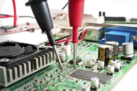
In-Circuit Testing (ICT)
ICT is a testing technique that verifies the functionality of individual components on a PCB. It involves using a bed-of-nails fixture to make electrical contact with specific test points on the board. The fixture is connected to a test system that applies stimuli and measures the response of the components.
ICT can detect:
– Short circuits
– Open circuits
– Incorrect component values
– Missing or incorrect components
– Incorrect Component orientation
ICT is an effective way to detect defects early in the manufacturing process, as it can test components before the board is fully assembled.
Flying Probe Testing
Flying probe testing is an alternative to ICT for low-volume production or prototypes. Instead of using a bed-of-nails fixture, flying probe testers use movable probes to make contact with test points on the PCB. The probes can be programmed to test specific components or net lists.
Flying probe testing offers several advantages over ICT:
– No need for custom test fixtures
– Flexibility to test different board designs
– Ability to test hard-to-reach components
– Lower setup costs for low-volume production
However, flying probe testing is generally slower than ICT and may not be suitable for high-volume production.
Functional Testing
Functional testing verifies that the assembLED PCB performs according to its intended design and specifications. It involves applying input signals to the board and measuring the output response. Functional testing can be performed at various levels, such as:
– Component level
– Sub-assembly level
– System level
Functional testing typically requires custom test fixtures and software to simulate the operating conditions of the device. It can detect defects such as:
– Incorrect component functionality
– Signal integrity issues
– Timing or synchronization errors
– Incorrect output responses
Functional testing is often performed after the PCB has passed other testing stages, such as AOI, ICT, or flying probe testing.
Boundary Scan Testing
Boundary scan testing, also known as JTAG (Joint Test Action Group) testing, is a technique used to test the interconnections between digital components on a PCB. It involves using a special test access port (TAP) on the components to control and observe the state of the input and output pins.
Boundary scan testing can detect:
– Short circuits
– Open circuits
– Stuck-at faults
– Incorrect component orientation
– Defective or missing components
Boundary scan testing requires that the components on the PCB support the JTAG standard (IEEE 1149.1). It is particularly useful for testing complex digital circuits, such as microprocessors, FPGAs, and ASICs.
Burn-In Testing
Burn-in testing is a technique used to identify early-life failures in electronic components and assemblies. It involves subjecting the PCB to elevated temperatures and electrical stresses for an extended period, typically several hours or days. The goal is to accelerate the aging process and reveal defects that may not be detected by other testing methods.
Burn-in testing can detect:
– Component degradation
– Solder joint failures
– Intermittent faults
– Temperature-related issues
Burn-in testing is often performed on a sample basis, as it can be time-consuming and costly to test every PCB.

PCBA Testing Techniques
PCBA testing techniques are similar to PCB testing techniques, but they focus on the assembled board rather than individual components. Some common PCBA testing techniques include:
Functional Testing
Functional testing of PCBAs is similar to functional testing of PCBs, but it may involve more complex test scenarios and input/output signals. The goal is to verify that the assembled board functions according to its design specifications and meets the required performance criteria.
In-Circuit Testing (ICT)
ICT can also be used to test PCBAs, but the test fixtures and programs may need to be modified to accommodate the assembled components. ICT can detect defects such as:
– Incorrect component values
– Missing or incorrect components
– Short circuits
– Open circuits
Flying Probe Testing
Flying probe testing can be used to test PCBAs, particularly for low-volume production or prototypes. The probes can be programmed to test specific components or net lists on the assembled board.
Boundary Scan Testing
Boundary scan testing can be used to test the interconnections between digital components on a PCBA. It requires that the components support the JTAG standard and that the test access port (TAP) is accessible on the assembled board.
Environmental Testing
Environmental testing is used to verify that the PCBA can withstand the expected operating conditions, such as:
– Temperature extremes
– Humidity
– Vibration
– Shock
Environmental testing may involve subjecting the PCBA to accelerated stress conditions to simulate long-term use and identify potential failures.

Advantages and Disadvantages of Different Testing Techniques
Each PCB and PCBA testing technique has its advantages and disadvantages. The choice of testing technique depends on various factors, such as:
– Board complexity
– Production volume
– Available resources
– Required test coverage
– Cost and time constraints
Here is a comparison of some common testing techniques:
| Testing Technique | Advantages | Disadvantages |
|---|---|---|
| Visual Inspection | – Low cost – Quick and simple – Can detect obvious defects |
– Subjective and prone to human error – Limited defect coverage – Not suitable for hidden or internal defects |
| Automated Optical Inspection (AOI) | – High speed and throughput – Consistent and objective – Can detect a wide range of defects |
– High initial cost – Limited to surface defects – May require programming and setup |
| X-Ray Inspection | – Can detect internal defects – Suitable for complex packages (e.g., BGA, flip-chip) – Non-destructive |
– High cost – Requires skilled operators – May have limited defect coverage |
| In-Circuit Testing (ICT) | – Can detect a wide range of defects – Suitable for high-volume production – Can test individual components |
– Requires custom test fixtures – Limited to accessible test points – May not detect functional defects |
| Flying Probe Testing | – Flexible and adaptable – No need for custom fixtures – Suitable for low-volume production |
– Slower than ICT – Limited to accessible test points – May not detect functional defects |
| Functional Testing | – Verifies overall functionality – Can detect defects not found by other methods – Ensures product quality and performance |
– Requires custom test fixtures and software – May be time-consuming and costly – Limited defect diagnosis capabilities |
| Boundary Scan Testing | – Can test complex digital circuits – Suitable for high-density boards – Can detect interconnect defects |
– Requires JTAG-compliant components – Limited to digital circuits – May require additional hardware and software |
| Burn-In Testing | – Can detect early-life failures – Identifies temperature-related issues – Improves product reliability |
– Time-consuming and costly – May not detect all defects – Typically performed on a sample basis |
Frequently Asked Questions (FAQ)
1. What is the difference between PCB and PCBA testing?
PCB testing focuses on testing the bare board and individual components, while PCBA testing involves testing the fully assembled board with all components soldered in place.
2. Is it necessary to perform all testing techniques on every PCB or PCBA?
No, the choice of testing techniques depends on various factors, such as board complexity, production volume, and required test coverage. Manufacturers often use a combination of testing techniques to ensure the quality and reliability of their products.
3. Can PCB testing techniques detect all types of defects?
While PCB testing techniques can detect a wide range of defects, no single technique can detect all possible defects. That’s why manufacturers often use a combination of testing techniques to achieve the desired test coverage.
4. How much does PCB testing cost?
The cost of PCB testing varies depending on the testing techniques used, the complexity of the board, and the production volume. In general, automated testing techniques like AOI and ICT have higher initial costs but can be more cost-effective for high-volume production. Manual testing techniques like visual inspection and flying probe testing may be more cost-effective for low-volume production or prototypes.
5. What are the industry standards for PCB and PCBA testing?
There are several industry standards and guidelines for PCB and PCBA testing, such as:
– IPC-A-610: Acceptability of Electronic Assemblies
– IPC-6012: Qualification and Performance Specification for Rigid Printed Boards
– IPC-J-STD-001: Requirements for Soldered Electrical and Electronic Assemblies
– IEEE 1149.1: Standard for Test Access Port and Boundary-Scan Architecture
These standards provide guidance on testing methods, acceptance criteria, and quality requirements for PCBs and PCBAs.
Conclusion
PCB and PCBA testing are critical processes in the manufacturing of electronic devices. By employing various testing techniques, manufacturers can ensure the quality, reliability, and functionality of their products. Each testing technique has its advantages and disadvantages, and the choice of technique depends on various factors such as board complexity, production volume, and required test coverage.
As the electronics industry continues to evolve, new testing technologies and methods are being developed to address the challenges of increasingly complex and high-density boards. Manufacturers must stay up-to-date with the latest testing techniques and industry standards to remain competitive and meet the demands of their customers.
By implementing a comprehensive testing strategy that includes a combination of visual inspection, automated optical inspection, X-ray inspection, in-circuit testing, flying probe testing, functional testing, boundary scan testing, and burn-in testing, manufacturers can achieve the highest levels of quality and reliability in their PCBs and PCBAs.


Leave a Reply