Introduction
Printed circuit boards (PCBs) are essential components in nearly all electronic devices today. As devices continue to get smaller and more complex, there is a growing need for PCBs that can accommodate higher densities of interconnects and components. This is where high-density interconnect (HDI) PCBs come in.
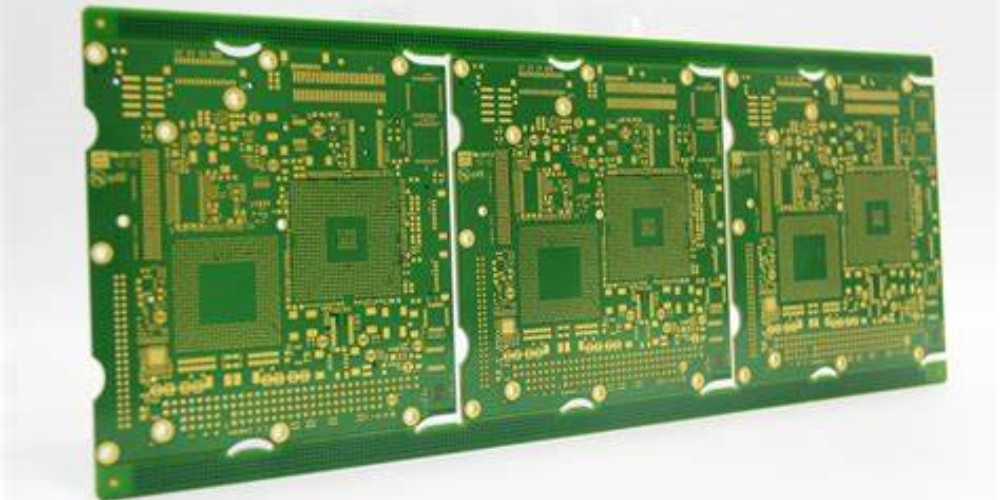
HDI PCBs utilize stacked microvias and fine lines/spaces to achieve interconnect densities beyond what is possible with standard PCBs. An 8 layer HDI PCB takes this a step further, providing even higher wiring densities and performance capabilities. In this guide, we will cover everything you need to know about 8 layer HDI PCBs including their design, fabrication, and applications.
What is an 8 Layer HDI PCB?
An 8 layer HDI PCB contains 8 conductive copper layers that are used to route signals and power/ground. Here is the typical stackup:
| Layer | Function |
|---|---|
| 1 | Signal |
| 2 | Ground |
| 3-6 | Signals |
| 7 | Power |
| 8 | Signal |
The key characteristics of an 8 layer HDI PCB are:
- Very fine lines and spaces – can be 5/5 mil and under
- Microvias with diameters as small as 0.15mm
- Stacked microvias for interconnection between layers
- High interconnect density > 200,000 holes/m2
- Thin dielectric materials for tightly spaced layers
- Tight impedance control for high speed signals
- Minimum finished thickness around 1.6mm
This combination of thin dielectrics, microvias, and fine features allows routing traces much more compactly to achieve a higher wiring density compared to standard PCBs. Components can also be placed closer together.
Applications of 8 Layer HDI PCBs

The capabilities of 8 layer HDI PCBs make them well suited for the following types of products:
- Smartphones – The small yet powerful integrated circuits in smartphones require a densely wired PCB to interconnect all components. HDI allows fitting more connections in the tight space.
- Wearable technology – Fitness bands, smart watches, and other wearables need to be lightweight and compact. Thin, multilayer HDI PCBs help minimize size and weight.
- Internet of Things (IoT) devices – Many IoT nodes are compact in size but require adequate wiring for sensors, microcontrollers, wireless modules etc. HDI is useful here.
- High speed electronics – Tight impedance control and thin dielectrics in HDI PCBs help maintain signal integrity at high frequencies for networking gear and test equipment.
- High pin count BGAs – Large ball grid array (BGA) packages can have 500-1000 pads underneath. HDI allows routing these effectively.
- RF boards – Radio frequency boards with sensitive analog and digital signals benefit from the dense, controlled routing of HDI PCBs.
In essence, any application where a standard 4-6 layer PCB does not provide adequate wiring density and high speed performance can utilize an 8 layer HDI PCB to meet design requirements.
Design Considerations for 8 Layer HDI PCBs
Designing an 8 layer HDI PCB requires special considerations compared to standard multilayer boards:
Layer Stackup
The layer stackup must be planned to provide adequate signal routing layers while balancing requirements for power delivery and shielding. A typical 8 layer HDI stackup was shown previously. Important guidelines are:
- Minimize number of dielectric materials to simplify fabrication and DfM
- Place core power and ground layers adjacent for decoupling
- Arrange signal layers for optimum breakout routing from BGAs/chips
- Control impedance with thin, consistent dielectric materials
Routing and Spacing
The microvia capabilities and fine features of HDI technology allow very dense routing with 5 mil lines or under. However, certain minimum design rules must still be followed:
- Trace width/spacing limits based on board shop capabilities
- Limit vias under BGA pads to avoid distortion during lamination
- Maintain minimum annular ring width for reliable microvias
- Allow slightly larger spacings around high speed traces
Microvia Stacking
A key benefit of HDI PCBs is stacked microvias which enable connections between non-adjacent layers with just one via hole. This minimizes routing congestion. Some guidelines for stacked microvias:
- Limit maximum stack height (e.g. 6-8 layers) based on aspect ratio
- Arrange stacks in a staggered pattern to maximize pull strength
- Avoid placing microvia stacks under small BGA pads
Controlled Impedance Routing
Many signals in high speed applications require controlled impedance traces with matched lengths. This involves:
- Selecting dielectric materials to achieve target impedance (50-100 ohms typical)
- Specifying trace width based on chosen stackup
- Controlling etchback regions when compensating trace lengths
Panel Utilization
HDI PCBs should follow layout practices to maximize the number of boards per panel:
- Arrange boards in a staggered pattern or “stepped” array
- Maintain similar board sizes within a panel when possible
- Allow for sufficient rails and break tabs between boards
- Optimize individual board shape for material utilization
DFM Practices
Following design for manufacturing (DFM) guidelines will minimize fabrication issues:
- Avoid acute angles between traces when possible
- Include teardrop pads at solder mask-plane interface
- Follow minimum hole sizes for microvias
- Allow adequate spacing around board profile
Paying attention to these considerations during layout will help in achieving a high yield and reliable HDI PCB. Collaboration with the board shop is also recommended to optimize the design.
Fabrication Process for 8 Layer HDI PCBs
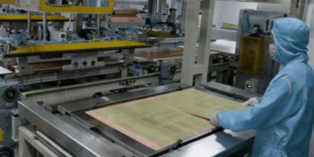
The fabrication of multilayer HDI PCBs relies on specialized processes to construct the fine features and microvias. Here is a simplified overview of the key fabrication steps:
- Inner layer production – Inner layer cores are processed starting with an RF laminate material clad with copper on both sides. Circuitry patterns are etched on each layer.
- Oxide treatment – The inner layer cores undergo an oxide treatment to improve adhesion with the prepreg materials.
- Layup – The inner cores, prepreg dielectric, and outer foils are precisely laminated together in a press under heat and pressure. Alignment is critical.
- Via formation – Microvias are drilled with laser or mechanical drills. Copper is plated to form the interconnections.
- Outer layer processing – Final circuitry patterns on the outer layers are etched to complete the conductive layers.
- Solder mask & legend printing – Solder mask is applied for soldering protection. Legends aid during assembly.
- Final metal finish – An immersion gold, ENIG, or other surface finish protects the exposed copper traces.
- Panel singulation – The individual PCBs are routed from the large panel. Break tabs may assist separation.
- Quality inspection – Electrical testing and optical inspection ensure the PCBs function as designed.
The raw board quality and reliability depend heavily on the fabrication process capabilities. Work with a high quality partner to produce your HDI PCBs.
Cost Comparison to Standard Multilayer PCBs
HDI PCBs provide enhanced capabilities, but generally at a higher cost compared to standard multilayers. Here is a rough comparison of cost factors:
| Parameter | Standard Multilayer | HDI PCB |
|---|---|---|
| Layer count | 4-6 layers | 6-8 layers |
| Minimum line/space | 6/6 mil | 3/3 mil or under |
| Minimum microvia diameter | 8-10 mils | 5-6 mils |
| Layer alignment | Basic | High precision |
| Materials | Standard FR-4 | High frequency laminates |
| Fabrication processes | Standard | Laser drilling, oxide treatment |
| Testing requirements | Basic electrical | Extensive HDI testing |
| Cost per area | Lower | 2-4X higher |
The advanced materials, tightly toleranced processes, and testing requirements of HDI PCBs lead to their higher fabrication costs. However, the benefits in miniaturization, performance, and reliability offset the pricing premium in most cases.
Buying and Design Guidelines for 8 Layer HDI PCBs
Here are some key guidelines when procuring and designing 8 layer HDI PCBs:
- Select a high quality fabricator with proven HDI capabilities
- Engage the vendor early in the design process for DFM feedback
- Understand the vendor’s HDI design rules and capabilities
- Leave adequate time for fabrication based on order quantity
- Utilize design software with extensive HDI and high speed features
- Simulate routing congestion with internal trace layers
- Follow sound layout practices for dense HDI routing
- Perform thorough design reviews before releasing to fab
- Test PCBs completely after fabrication including HDI defects
By partnering with the right supplier and following good design practices, you can take full advantage of the benefits of 8 layer HDI technology.
FAQ
Here are some frequently asked questions about 8 layer HDI PCB technology:
Q: What are the typical board thickness values for an 8 layer HDI PCB?
A: The finished thickness of a typical 8 layer HDI board is around 1.6mm. Inner layer dielectric thickness is commonly around 0.075mm.
Q: Can 8 layer HDI boards incorporate buried and blind vias?
A: Yes, laser drilling enables creating blind and buried vias in HDI boards to optimize layer transitions. This helps maximize routing channels.
Q: What are the main failure modes to watch out for with HDI PCBs?
A: Potential failure modes include microvia cracking or separation, poor adhesion between layers, imperfect lamination, and insufficient pad strength under components. Proper design and fabrication minimizes these risks.
Q: What are the advantages of outsourced assembly for HDI boards?
A: Outsourcing to an expert assembly provider allows utilizing specialized processes like microvia filling and advanced soldering techniques. This helps maximize yields.
Q: Can flex PCBs utilize HDI technology?
A: Yes, fine features and microvias can be incorporated in flex PCBs to achieve similar interconnect density benefits as rigid HDI circuit boards.


Leave a Reply