Introduction
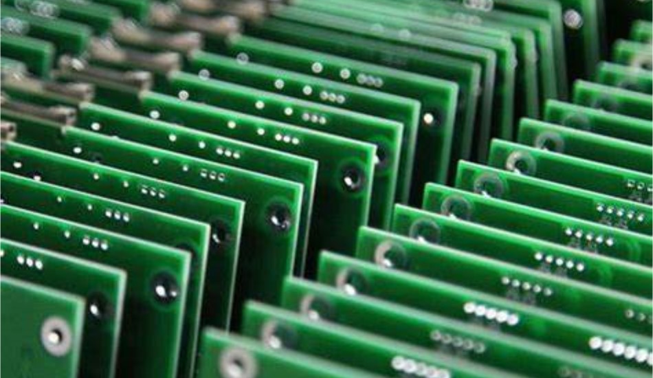
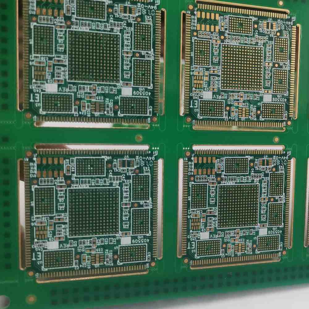
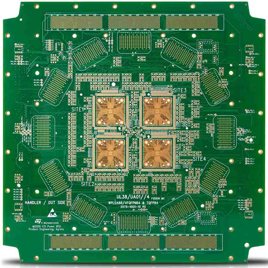
Printed circuit boards (PCBs) are essential components in most modern electronic devices. As products become more complex and miniaturized, there is an increasing need for PCBs with more layers to accommodate higher component density and intricate circuit routing. 6 layer PCBs provide the interconnectivity and signal integrity required for today’s high-speed and high-frequency applications. However, not all PCB manufacturers are equipped to reliably produce multi-layer boards. Choosing the right 6 layer PCB manufacturing partner is crucial to ensuring your product’s functionality and quality. This article provides guidance on selecting the best 6 layer PCB fabrication vendor for your specific needs.
Key Considerations for a 6 Layer PCB Manufacturer
When evaluating potential 6 layer PCB suppliers, keep the following important criteria in mind:
Technology and Equipment
The manufacturer should utilize advanced fabrication equipment and processes tailored for multi-layer PCBs. This includes:
- High-precision laser direct imaging (LDI) for fine line resolution and registration accuracy between layers
- Advanced drilling equipment such as CNC laser drills for high hole quality
- Plating equipment capable of achieving uniform copper thickness across 6 layers
- Layer alignment systems to minimize layer shifting during lamination
- Rigorous quality inspection systems
They should be able to reliably produce 6 layer boards down to at least 4 mil line/space and 1 mil hole size.
Materials and Capabilities
- The manufacturer should offer a wide range of UL-approved base materials, including common FR-4, high frequency RF materials, and high speed materials like PTFE.
- They should be able to handle board thicknesses up to 2.4 mm or more.
- Scrupulous process controls for materials sourcing, inventory, and storage.
- Flexible and user-friendly sourcing of components, inventory management, and assembly integration services.
Quality and Certifications
The company should have a robust quality management system and ISO 9001 certification at a minimum. More advanced certifications such as AS9100 demonstrate technical expertise.
Sample quality inspection rate should be at least 2-4% with comprehensive testing. They should be willing to share detailed quality control procedures and data.
Reliability and Consistency
Consistency and repeatability is critical for 6 layer PCBs. Ensure the manufacturer has a proven track record of on-time delivery and quality for multi-layer PCB production in relevant volumes.
Ask for customer references and samples of previous 6 layer boards they produced. Verify their product yield rate and history of meeting specifications.
Top 6 Layer PCB Manufacturers
Here are a few reputable 6 layer PCB manufacturers operating globally that meet the criteria discussed above:
Advanced Circuits
- Location: Colorado, USA
- Capabilities: 6-36+ layer PCBs; 4 mil line/space; 0.4 mm vias; panel sizes up to 33 x 47 inches; 1 oz to 6 oz copper; Al base material
- Quality certifications: ISO 9001:2015; ITAR Registered; IPC 6012 Class 3, Class 3A
- Quickturn prototyping available in as fast as 24 hours
- Production volumes scalable up to 5000 boards/week
Sunstone Circuits
- Location: Oregon, USA
- Capabilities: 6-24 layer PCBs; flex and rigid-flex; 2 mil line/space; 1 mil microvias; 1 oz to 10 oz copper; delivers in 2-10 days
- Quality certifications: ISO 9001:2015; ITAR; IPC 6012 Class 2 and 3; certified UL lab; MIL-PRF-31032; IPC 6018
Sierra Circuits
- Locations: California and Nevada, USA
- Capabilities: 6-30 layer PCBs; 3 mil trace/space; 0.5 mm holes; panel size up to 35 x 47 inches
- Quality certifications: ISO 9001:2015; ITAR; IPC 6012 Class 2 and 3; IPC/WHMA-A-620; J-STD-001
PCBWay
- Location: China
- Capabilities: 6-36 layer circuit boards; SMT stencil and PCB assembly; responds in 6-24 hours; lower minimum order quantities
- Quality certifications: ISO 9001:2015; IPC 6012;IPC-A-600; TS16949;UL approval available
WellPCB
- Location: China
- Capabilities: 6-32 layer PCBs; multilayer HDI boards; panel size up to 35.4 x 47.2 inches
- Quality certifications: ISO 9001; IATF 16949; IPC, UL, SGS, TUV approvals available
- Rapid prototyping service delivers in 2 days
ALLPCB
- Location: China
- Capabilities: 6-36 layer PCBs; 5 mil trace/space; panel size up to 34 x 62 inches
- Quality certifications: ISO 9001:2015; IATF 16949:2016; ISO 14001:2015
- Accepts orders from prototype to mid-volume production
Key Questions to Ask Potential Manufacturers
When sourcing a 6 layer PCB supplier, make sure to clearly communicate your product needs and specifications. Ask questions such as:
- What 6 layer stackups do you offer? Can you manufacture the layer count and thickness I need?
- What is the minimum trace/space you can achieve? What design rules do I need to comply with?
- What materials, finishes, thicknesses, and panel sizes are available?
- Can you meet my lead time requirements for prototyping and volume production?
- Do you have in-house engineering support for design reviews and DFM?
- What testing, inspection, and quality certifications can you provide? What are your quality standards?
- Can you supply any samples of 6 layer PCBs you produced previously?
- What technical capabilities and expertise for 6 layer boards does your team have?
- Do you provide assembly and other value-added services?
Carefully screening potential 6 layer PCB production partners using these criteria will help ensure you select the right match for your product.
Main Factors that Impact Costs of 6 Layer PCBs
Like any complex manufacturing process, many variables factor into the costs of producing 6 layer printed circuit boards. Some of the main drivers include:
Board Size
Larger PCB panels require more materials and processing, increasing costs. Standard sizes can be more economical.
Layer Count
Base price increases with more layers due to additional materials, lamination cycles, and complexity.
Design Complexity
More complex circuit designs require tighter tolerances, more drill holes, and advanced capabilities – raising costs.
Board Thickness
Thicker boards use more materials. 1.6 mm is standard; above 2.4 mm often incurs premiums.
Order Volume
Higher volumes provide economies of scale and lower cost per board. Prototypes have higher costs.
Lead Time
Rushed delivery times often command premium pricing. Standard lead times around 2 weeks are most economical.
Special Requirements
Uncommon materials, finishes, certifications, testing, etc. can drive up costs.
Keeping design requirements reasonable and ordering in sufficient volumes are key strategies for cost management. Discuss these factors openly with your PCB manufacturer.
Conclusion
This overview summarizes the essential capabilities and qualifications to look for in a reliable 6 layer PCB manufacturing partner. A reputable supplier with proven technological expertise in multi-layer boards, robust quality systems, and customer-focused service will be critical to the success of your advanced PCB fabrication project. Asking the right questions during the vetting process is key to finding the best match.
Frequently Asked Questions
Q: What are the main benefits of 6 layer PCBs?
A: 6 layer boards provide more routing channels than 2 or 4 layer PCBs to accommodate higher component densities. They allow for separating power and ground planes to reduce noise. The additional layers also enable shorter trace lengths and controlled impedance for better high frequency performance.
Q: What are typical applications for 6 layer PCBs?
A: 6 layer boards are commonly used in products like telecommunications equipment, industrial electronics, medical devices, automotive electronics, and advanced consumer products. The complexity supports radio frequencies up to 5Ghz.
Q: What design software do I need for a 6 layer board?
A: Advanced PCB CAD software tools like Altium Designer, Cadence Allegro, and Zuken CR-8000 are typically used. They have robust multilayer board functionality and design rule checking to help you design effectively for manufacturability.
Q: Can vias be used to route between inner layers?
A: Yes, blind and buried vias are used in 6 layer boards to interconnect between internal layers without having to drill through the entire board stackup. This helps optimize routing and density.
Q: How long does 6 layer PCB manufacturing typically take?
A: For an efficient manufacturer utilizing advanced equipment, typical production lead times range from 5 days up to 4 weeks depending on prototyping vs. volume production. Expedited orders can sometimes ship in 2-3 days.


Leave a Reply