
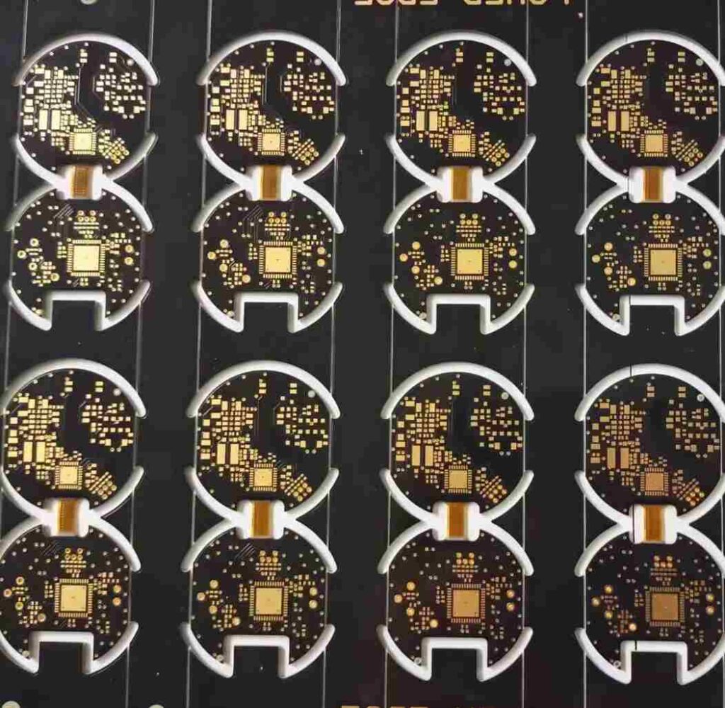
HDI (high-density interconnect) PCBs enable the miniaturization of electronics by packing more features into less space. As products like smartphones and wearables push the envelope with smaller, thinner, and lighter designs, many require advanced HDI PCBs with more than 40 layers to fit complex circuitry into tight confines.
52 layer HDI PCBs represent the leading edge of PCB technology. They can integrate fine lines, microvias, and other intricacies to optimize layout and routing in extremely dense packages. However, reliably producing 52 layer boards requires expertise in advanced manufacturing processes.
This article will cover how to pick the right 52 layer HDI PCB manufacturing partner to meet your needs.
Why Choose a 52 Layer HDI PCB?
HDI PCBs offer many benefits for space-constrained and complex designs:
Miniaturization
- More board layers allow higher component density with shorter traces for compact layouts.
Performance
- Fine features improve high-speed signal integrity.
- More layers enable separation of analog and digital signals to reduce interference.
Reliability
- Interlayer connections through microvias take up less space than through-hole vias.
- Microvias have lower inductance for cleaner power delivery.
For the most demanding applications like high-speed computing, aerospace systems, and cutting-edge consumer gadgets, 52 layer HDI PCBs provide the ultimate combination of small size and excellent electrical performance.
Key Considerations When Selecting a 52 Layer HDI PCB Manufacturer
Building ultra-high layer count PCBs requires significant expertise and capital investment. However, not all manufacturers have the capabilities or experience to reliably produce these advanced boards.
Here are key factors to evaluate when choosing a 52 layer HDI PCB fabrication partner:
Technology and R&D
- Leading-edge equipment for processes like laser direct imaging (LDI) and automated optical inspection (AOI).
- Ongoing R&D in advanced PCB materials and manufacturing methods.
Engineering Expertise
- Knowledgeable engineering team that can provide design review and DFM analysis.
- Experience fabricating and troubleshooting issues with high layer count boards.
Quality Systems
- Certifications like ISO 9001 and AS9100D to validate capabilities and quality management.
- Comprehensive quality assurance procedures at every step.
Capacity Scalability
- Equipment capacity to handle required production volumes.
- On-demand scalability to meet changing production needs.
Customer Service
- Dedicated customer support team for questions and issue resolution.
- Real-time order monitoring and production status updates.
Competitive Pricing
- Total costs competitive with other advanced PCB fabricators.
- Flexible pricing models like volume discounts.
Major 52 Layer HDI PCB Manufacturers in China
Many leading HDI PCB manufacturers capable of 52 layer boards are located in China. Large EMS companies like Foxconn and Flextronics have in-house PCB fabrication. There are also numerous specialized PCB makers pushing the envelope in HDI technology.
Here is an overview of major 52 layer HDI PCB manufacturers in China:
Top 10 HDI PCB Manufacturers in China
| Company | Location | Max Layers | Certifications |
|---|---|---|---|
| Shennan Circuits | Shenzhen | 100+ | ISO 9001, UL, IATF 16949 |
| LT Circuit | Zhuhai | 100+ | ISO 9001, AS9100D |
| Kinwong | Suzhou | 100+ | ISO 9001, ISO 13485 |
| WUS Printed Circuit | Kunshan | 100+ | ISO 9001, AS9100D |
| AT&S | Nanjing | 100+ | IATF 16949, AS9100D |
| Tripod Technology | Hubei | 100+ | ISO 9001, ISO 14001 |
| HannStar Board Corporation | Nanjing | 80+ | ISO 9001, IATF 16949 |
| ZDX | Guangzhou | 60+ | ISO 9001, ISO 13485 |
| Multi-Fineline Electronix | Suzhou | 60+ | ISO 9001, AS9100D |
| Ibiden | Shanghai | 60+ | IATF 16949, AS9100D |
This table summarizes key info on some of the major HDI PCB manufacturers in China that can produce 52+ layer boards, including their location, maximum layer count capability, and certifications.
Many hold advanced certifications like AS9100D for aerospace and defense work, demonstrating their process capabilities for ultra-high reliability applications. Leading manufacturers are investing heavily to push the boundaries of HDI technology even further.
Notable Advanced HDI PCBs from China
Here are some examples of advanced HDI PCBs produced by manufacturers in China:
- 105 layer HDI PCB – Shennan Circuits produced a 105 layer HDI PCB with 0.5 mm thickness for a 5G telecom module.
- 100 layer PCB – WUS Printed Circuits fabricated a 100 layer board with 0.45 mm thickness and 150,000 microvias for a complex communications product.
- 76 layer HDI PCB – LT Circuit manufactured a 76 layer HDI board with 0.6 mm thickness and 250,000 microvias for a high-speed computing application.
- 64 layer HDI PCB – Kinwong built a 64 layer HDI board with 0.8 mm thickness featuring embedded impedance-controlled routing for aerospace avionics.
- 60 layer flex-rigid PCB – ZDX produced a 60 layer flex-rigid PCB just 0.6 mm thick for a wearable smart device.
These examples demonstrate the impressive layer counts and design intricacies that advanced Chinese PCB fabricators can reliably produce at volume today. Their expertise continues advancing steadily.
Evaluating Manufacturers’ HDI PCB Capabilities
Not all manufacturers touting “HDI PCB” capabilities can actually produce 52+ layer boards suitable for advanced applications. Here is how to dig deeper to evaluate their true expertise:
Questions to Ask
- What is your maximum achievable layer count? What is the thinnest board you can manufacture at 52+ layers?
- What are your minimum trace/space and microvia dimensions? Can you fabricate 2/2 L/S at 52 layers?
- What HDI stackups and materials do you offer? Do you support key RF materials like PTFE composites?
- What is your first-pass yield percentage for high layer count HDI PCBs? How do you verify yields?
- Can you provide examples of complex HDI boards you have mass produced?
Capabilities to Look For
- Layer counts of 80+ layers, with roadmap to 100+ layers
- 2-3 mil thick boards with 50+ layers
- Commercial production of 2/2 L/S traces and 1-2 mil microvias
- First-pass yields above 90% for multilayer boards
- Experience with advanced RF materials like LCP
Red Flags
- Vague claims of “HDI capabilities” without specifics on layer counts, L/S, etc.
- Limited experience with complex layer counts above 16 layers
- Quoting extremely long lead times of 8+ weeks for advanced HDI
- Unwillingness to provide references or examples of high layer count boards
Taking a detailed look at manufacturers’ actual commercial capabilities will help you determine who can truly deliver the 52+ layer HDI PCB technology you require today.
Detailed Comparison of 5 Top 52 Layer PCB Manufacturers in China
Here is an in-depth side-by-side look at 5 of China’s leading 52+ layer HDI PCB manufacturers:
Major 52 Layer HDI PCB Manufacturers in China Comparison
| Manufacturer | Max Layers | Min. Spacing | DFM Analysis | First-Pass Yield | Lead Time |
|---|---|---|---|---|---|
| Shennan Circuits | 105+ | 0.5/0.5 mm L/S | Yes, extensive | >95% (HDI) | 2 weeks |
| WUS PCB | 100+ | 0.5/0.5 mm L/S | Yes | >90% (multilayer) | 3 weeks |
| Kinwong | 100+ | 0.3/0.3 mm L/S | Yes | >90% (HDI) | 4 weeks |
| Hannstar Board | 80+ | 0.3/0.3 mm L/S | Limited | N/A | 6 weeks |
| ZDX | 65+ | 0.4/0.4 mm L/S | Yes | >85% (HDI) | 4 weeks |
This comparison examines key criteria like maximum layer counts, smallest trace/space dimensions, design analysis capabilities, yields, and lead times.
It provides a quick snapshot of how the top players’ offerings differ. You can use these data points to narrow down the list based on which specs are most important for your specific 52+ layer HDI PCB design needs.
Recommended Manufacturers
Based on the table above, these three manufacturers stand out as strong choices for advanced 52+ layer HDI PCB production:
- Shennan Circuits – With 105 layer capability and excellent yields, they are a top choice for leading-edge HDI.
- WUS PCB – Their 100 layer capacity and rapid turnaround gives them a competitive edge.
- Kinwong – With 8-week lead times but tight trace dimensions and solid yields, they offer a balance of capabilities.
Starting your vendor selection process here provides a short list of impressive 52 layer HDI PCB manufacturing partners to evaluate further.
Key Takeaways on Selecting a 52 Layer PCB Manufacturer
Here are some final recommendations when choosing a 52 layer HDI PCB fabrication partner:
- Focus your search on manufacturers in China with proven high layer count expertise.
- Thoroughly investigate capabilities – don’t just rely on marketing claims.
- Prioritize manufacturers with strong engineering collaboration and DFM analysis.
- Validate quality management with certifications and customer references.
- Require first-article prototypes to inspect process execution firsthand.
- Choose suppliers with scalability to meet future growth in production volumes.
By carefully vetting manufacturers’ actual technical capabilities, service offerings, and production chain maturity, you can find the right partner to bring your advanced 52 layer HDI PCB from design through high-volume fabrication.
Frequently Asked Questions
Here are answers to some common questions about specifying and manufacturing advanced 52 layer HDI PCBs:
What design rules and stackup requirements should I follow for a 52 layer HDI PCB?
Follow your manufacturer’s specific design rules closely, as they may vary. In general, minimize traces below 5 mil width, allow at least 2 mil spacing between traces, use microvias under 2 mil diameter, and work with your manufacturer on optimal stackup for signal integrity. High-speed signals may require impedance controlled routing.
What thickness should I expect for a minimum 52 layer count PCB?
You can achieve 52 layers in approximately 2.4 to 3.2 mm thickness, though high-end manufacturers can reach 2 mil layer thicknesses to potentially minimize thickness further. Very thin PCBs may require additional considerations like special handling.
Can I bury controlled impedance traces between layers on my 52 layer board?
Yes, high-end manufacturers can build impedance-controlled routing layers between signal layers connected by microvias to maintain integrity of matched trace impedances. This enables proper performance of microwave, high-speed digital, etc.
How long does full fabrication cycle time take for a 52 layer board?
From design handoff to parts delivery, allow 4-6 weeks for fabrication. First-article builds may take 1-2 weeks longer for iterative prototyping to finalize layers, microvias, etc. Very complex boards may need 8+ weeks. Discuss timeline with your manufacturer.
How much more will a 52 layer HDI PCB cost versus a 16 layer board?
Expect approximately 4X the cost for a 52 layer board over a 16 layer design, based on increased layer count, thinner layers, and smaller features. However, reduced size from greater miniaturization can offset increased fabrication costs.
Conclusion
As products require continued innovation in electrical and physical design, advanced 52 layer HDI PCB fabrication enables packing more functionality into ever-shrinking packages. Today’s leading manufacturers in China are pushing the boundaries of layer count, feature size, and electrical performance to meet these needs. By selecting suppliers with proven expertise in building the most complex PCBs, designers can reliably turn cutting-edge concepts into manufacturable products.


Leave a Reply