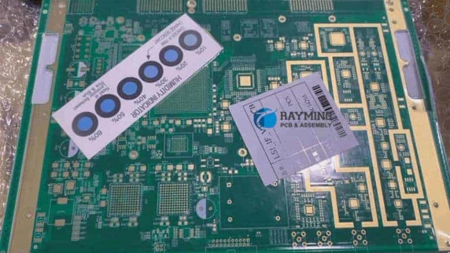
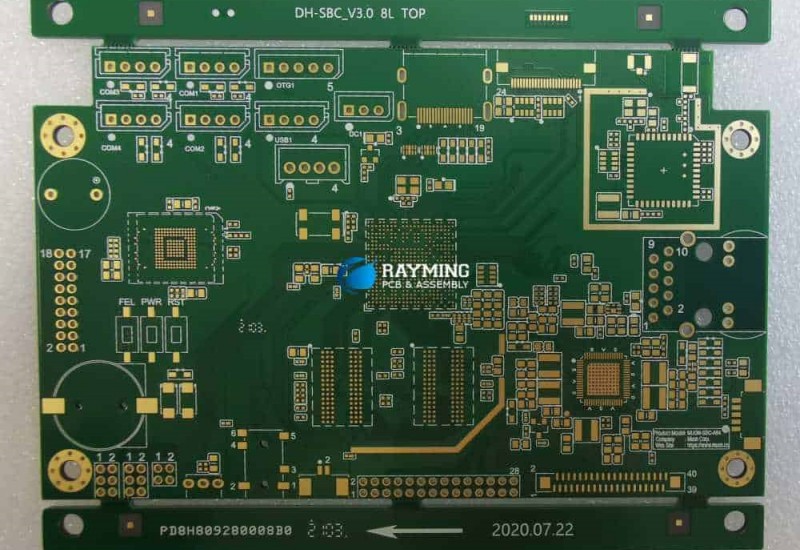
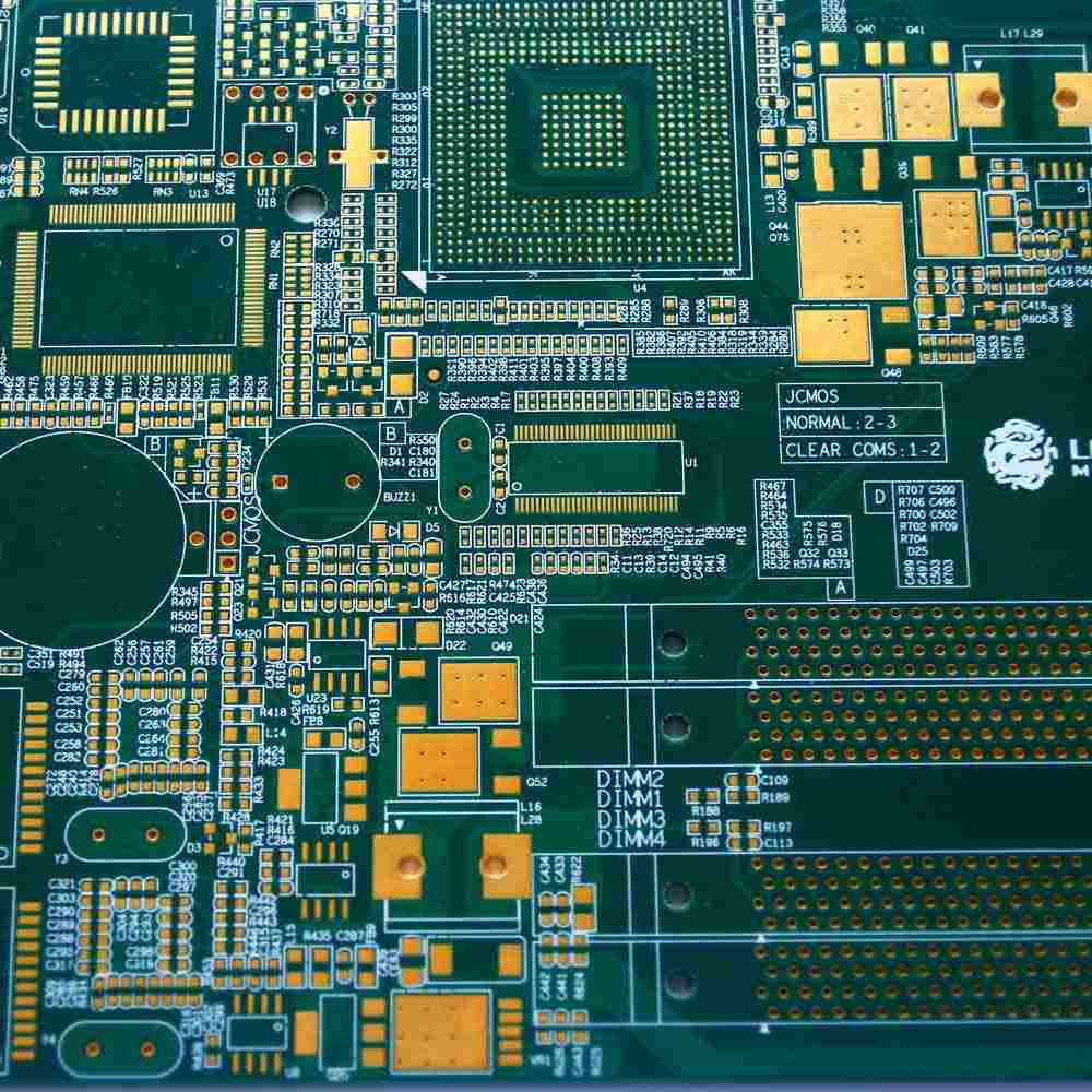
High density interconnect (HDI) printed circuit boards (PCBs) with 44 layers or more provide an extremely dense interconnect solution for advanced electronic devices. As components and functions continue getting smaller and more complex, PCBs must adapt to accommodate higher input/output (I/O) counts in limited spaces. Manufacturers capable of reliably producing multilayer HDI PCBs play a critical role enabling ongoing miniaturization and performance improvements.
Benefits of 44+ Layer HDI PCBs
Moving to 44 layers or more provides numerous benefits for complex, compact PCBs:
Increased Routing Channels
With more layers, PCB designers have more routing channels available to connect components. This enables higher interconnect density and the ability to route traces for high pin count devices.
Smaller Vias
HDI manufacturing processes allow the use of microvias, which take up less space than traditional vias. More layers with microvias provides more vertical routing options without sacrificing as much board real estate.
Embedded Passives
Some 44+ layer HDI boards embed passive components like resistors and capacitors within the PCB layers. This saves space compared to surface mount passives while also reducing assembly costs.
Reduced EMI
Proper use of multiple board layers effectively isolates signals to prevent interference and crosstalk. This becomes increasingly important with faster signal edge rates.
Lower Impedance Power Delivery
Power distribution across more layers drops impedance, enabling cleaner power delivery to ICs even at high currents. This helps stabilize power integrity.
High Frequency Support
Thinner dielectrics between layers support higher frequency signals with tightly controlled impedances. HDI boards routinely achieve line-space traces below 100 μm.
Construction of 44+ Layer HDI PCBs
Constructing HDI PCBs with over 40 layers requires specialized materials, processes, and equipment to meet the tight tolerances involved. Here are some construction details:
Layer Stackup
The layer stackup defines the sequence of dielectric, copper foil, and core materials building up the board. Stackups balance parameters like thickness, dielectric constant, and materials.
Typical core thicknesses range from 0.05 to 0.2 mm for sub-100 μm lines and spaces. Most designs use thinner dielectrics on outer layers and thicker cores internally.
Materials
Epoxy glass composites still comprise the core materials for most HDI boards. These provide mechanical support. Popular options include FR-4, BT, and various ceramics.
Dielectrics include traditional epoxy, polyimide, cyanate ester, and other high performance polymers. These maintain insulation between copper layers.
Copper foils fall into standard electrodeposited and treated rolled types. Very fine lines use electrodeposited copper.
Via Structures
Blind and buried microvias with diameters below 150 μm electrically connect surface layers to internal layers. Their small size allows high density routing.
Skip vias stitch together several internal layers for even denser vertical interconnections. Sequential lamination combines layers around drilled skip vias.
Pagination
Producing individual thin cores then “paginating” them together into a thick multilayer stack enables tighter process control. This helps minimize registration issues between layers to hold fine tolerances.
Advanced Processes
Specialized processes like plasma treatment and surface finishes prepare materials for lamination while enhancing adhesion and reducing stresses. Tight process controls ensure reliability.
Leading 44 Layer PCB Manufacturers
A number of leading PCB manufacturers based in China and Taiwan boast extensive experience producing advanced HDI boards in high volumes:
Shennan Circuits
- One of the pioneering HDI PCB producers in China
- Capabilities up to 60-layer boards
- Stackup construction expertise
- Mass production volumes
- ITAR registered
Kinwong Electronic
- Strong in RF designs up to mmWave
- Builds flex-rigid boards with 30+ layers
- Specializes in miniaturization
- Design support services
- Facility in Richardson, Texas
TTM Technologies
- Among the technology leaders globally
- Produces extreme HDI boards over 70 layers
- Advanced process expertise
- Facilities in Asia and North America
- ITAR and AS9100 certified
Tripod Technology
- Major Taiwan-based manufacturer
- Long history producing multilayer boards
- Significant capacity across Asia
- Leading HDI and IC substrate supplier
- Rigorous quality systems
Unimicron Technology
- One of Taiwan’s largest PCB producers
- High density interconnect focus
- Supplies leading electronics OEMs
- Global manufacturing footprint
- Process expertise in microvias
These manufacturers and others continue pushing HDI boundaries as densification demands increase. Their investments in advanced processes and equipment are essential for progress.
Key Factors When Selecting a 44 Layer PCB Manufacturer
Since PCBs form the foundation of electronics, selecting the right 44+ layer HDI PCB manufacturer is critical. Key factors to consider include:
Experience – Look for extensive knowledge working with cutting edge HDI designs and high layer counts. Evaluate their track record with leading customers.
Capabilities – Ensure the manufacturer can construct complex layer stackups and manufacture microvias below 100 μm. Ask about their minimum line widths and via diameters.
Quality – Examine process capabilities to ensure sufficiently tight tolerances. Review their quality certifications and systems. Conduct audits as warranted.
Volume – Assess production capacity and scalability for volume manufacturing. Ensure they can support eventual demand.
Services – Determine if the manufacturer provides value-added services like design support that will simplify development.
Logistics – Choose a manufacturer with facilities near your team to enable collaboration and accelerate delivery.
Selecting the right partner requires thorough vetting across these criteria. The increased complexity of high layer count HDI merits rigorous evaluation to mitigate program risks.
HDI PCB Technology Outlook
HDI technology continues evolving to pack greater functionality into smaller packages across a range of markets:
Increasing Layer Counts
Manufacturing processes constantly improve, enabling reliable production of PCBs with more layers. This provides designers enhanced routing flexibility. Layer counts beyond 100 layers could become practical for extremely complex designs.
Thinner Dielectrics
Using thinner dielectric materials between copper layers supports tighter trace geometries. Polymer dielectrics below 10 μm thick help construct high density interconnects on fine line PCBs.
Any Layer Microvias
Skip vias already stitch between some internal layers. Any layer microvias encompassing all layers would maximize vertical routing flexibility without performance penalties.
Embedded Actives and Passives
Embedding active components like logic dies and passive parts into package substrates will enhance electrical performance while saving space. This represents a major packaging evolution.
Advanced Materials
Materials research seeks improved dielectric properties and fabrication capabilities. Graphene and other novel materials may eventually enable breakthrough PCB performance.
In coming years 44+ layer HDI PCBs will continue gaining applications across computing, networking, aerospace, defense, automotive, and consumer markets as technology improvements further advantages.
Frequently Asked Questions
What are the key benefits of 44 layer PCBs?
Key benefits include increased routing channels, smaller vias, embedded passives, reduced EMI, lower power distribution impedance, and high frequency support. The additional layers provide more interconnect flexibility.
How are 44 layer HDI PCBs constructed?
Specialized layer stackups, thin dielectric materials, microvias, and advanced lamination processes enable construction. Tight process controls, precision drilling and alignment, and sequential pagination help achieve the high densities.
What types of products use 44 layer PCBs?
High density interconnects are found in products like high-end FPGAs, ASICs, GPUs, servers, switches, advanced radar and communications, aerospace avionics, and even some consumer devices. Their complexities benefit from more PCB layers.
What tolerances can HDI PCB manufacturers achieve?
Leading HDI manufacturers can reliably produce boards with line widths and spaces under 50 μm (2 mils), microvias below 100 μm (4 mils), and registration accuracy around 25 μm (1 mil). Electrical tolerances are also tightly controlled.
Does layer count keep increasing for HDI PCBs?
Yes, manufacturing processes continue improving to increase reliable layer counts. While 60-70 layers is currently practical, the substrate industry roadmap projects continuing growth. Boards could potentially reach over 100 layers for extremely complex future applications.


Leave a Reply