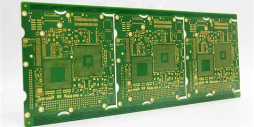
As printed circuit boards become more complex, high density interconnect (HDI) PCBs with large numbers of layers are increasingly required. 42 layer HDI PCBs enable intricate routing for advanced applications like 5G, automotive electronics, aerospace avionics, and medical devices. However, not all PCB manufacturers have the capabilities to reliably produce boards with so many layers. Choosing the right partner is key to getting high quality 42 layer HDI PCBs.
What are 42 Layer HDI PCBs?
HDI refers to boards with a higher interconnect density than standard PCBs. This is achieved by:
- Using thinner dielectric material between copper layers
- Smaller trace widths and spacing
- More layers
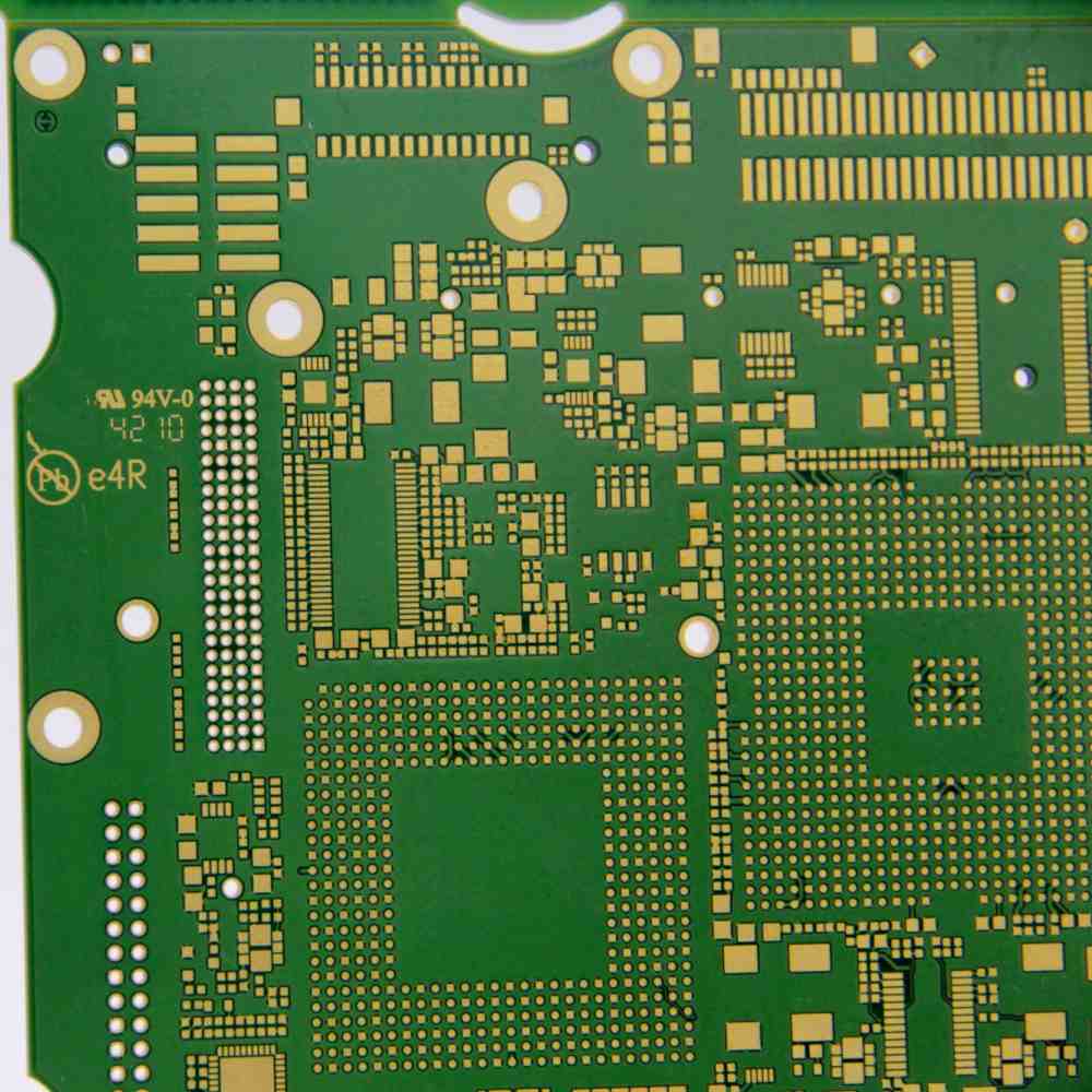
42 layer HDI PCBs integrate 42 conductive copper sheets separated by dielectric material. Vias make electrical connections between layers. With so many layers, complex designs with high component density and intricate routing can be realized without compromising on board space.
Key Features of 42 Layer HDI PCBs
- Extremely high interconnect density
- Up to 42 routing layers
- Trace/space down to 2/2 mils
- Laser cut microvias with 5-10 mil annular rings
- Stacked and staggered microvias
- Built-up dielectric layers down to 2 mils
- High component density on both sides
- Fine line traces and spaces
- High frequency applications up to 5G mmWave
- High speed signal transmission 10+ Gbps
- Power distribution in inner layers
- Embedded passives – resistors, capacitors
- Small overall board thickness 0.5-1.0mm
Applications of 42 Layer HDI PCBs
The capabilities of 42 layer HDI PCBs make them well suited for:
- 5G base stations and infrastructure
- Aerospace and defense electronics
- Automotive – ADAS, infotainment
- Medical imaging and diagnostics equipment
- High speed computing and network hardware
- Next generation smartphones and gadgets
- Any application requiring small size and high performance
Capabilities Required for 42 Layer HDI PCB Manufacturing

Building reliable PCBs with 42 layers is enormously complex compared to standard boards. Only manufacturers with advanced technical capabilities can successfully produce these boards without defects. Key requirements include:
Board Stackup Design
The board layer stackup must be meticulously engineered to balance signal integrity, power delivery, and heat dissipation. This includes selecting optimal dielectric materials, copper weights, and layer thicknesses. Simulation and modeling informs an optimal stackup.
Fabrication Process Control
42 layers of copper must be electrically isolated by thin dielectric layers with high precision. This requires excellent process control over lamination, laser drilling, plating, etching, oxide treatment, and AOI. Minor variations can cause defects.
Registration Accuracy
With 75-125μm vias spanning over 40 layers, even the slightest misalignment of layers during lamination can cause reliability issues. Tight registration tolerances must be maintained.
Advanced Testing and Inspection
Testing just the outer layers is insufficient for 42 layer boards. Rigorous electrical testing strategies combined with x-ray laminography, automated optical inspection (AOI), and acoustic microscopy are needed to validate function and catch defects.
Thermal Management
The laminate thickness and number of layers restricts heat dissipation. Thermal analysis should inform stackup design. Often, thermal vias, buried heat sinks, and backside metallization are used.
Miniaturization Techniques
To achieve a high component density, advanced miniaturization techniques are used:
- Microvias with 8-12 mil annular rings
- 0201 and 01005 passives
- 0.3mm to 0.15mm pitch BGAs
- High density wafer level packaging (WLP)
- Embedded discrete passives
What to Look for in a 42 Layer PCB Manufacturer?
Not every PCB factory can reliably produce 42 layer HDI boards. When selecting a manufacturing partner, consider the following:
Proven Capabilities
- Years of experience manufacturing 20+ layer HDI PCBs
- Demonstrated expertise with specific requirements: registration accuracy, HDI stacked microvias, fine line traces/spaces, lamination process, via formation/metallization, electrical testing.
- Qualification and certifications (AS9100, ISO9001, UL, IATF 16949)
Engineering Support
- Provide stackup design, documentation, and simulation services
- Thermal analysis and buried heat sink design assistance
- DFM input for optimal manufacturability
- Test development collaboration
Quality and Reliability
- Process and quality controls to minimize defects
- Comprehensive testing – bare board electrical, x-ray, AOI, C-SAM
- Analysis tools – SEM, XRF, C-SAM
- Contingency planning for continuity of supply
Advanced Equipment/Facilities
- High layer count multilayer lamination presses
- Laser direct imaging for fine features
- Registration analysis and tuning tools
- X-ray laminography for inner layer inspection
- Reliable AOI, test, and inspection systems
Reasonable Lead Times and Pricing
- Offer prototyping through production quantities
- Competitive pricing for high layer count boards
- Meet target lead times reliably
Top 42 Layer PCB Manufacturers
Many PCB factories claim high layer count capabilities but few can reliably deliver. Here are some of the leading manufacturers known for advanced HDI and multilayer boards.
TTPCB
TTM Technologies’ Asian divisions produce complex multilayer boards for defense, aerospace, networking, 5G infrastructure, and mobile applications. Their TTPCB site has extensive HDI and any-layer expertise.
NCAB Group
This European based manufacturer operates factories in China running advanced processes for HDI boards over 20 layers. Their China team has expertise in high density interconnects.
AT&S
This Austrian company has plants in China and India producing complex boards for automotive, industrial, and mobile clients. They are experienced in stacked microvias, blind vias, and other HDI techniques.
Unimicron
Known for ABF substrates, Unimicron also operates advanced multilayer and HDI facilities in Taiwan, Japan and China. Their technology spansocarospace, telecom, and networking.
Tripod Technology
One of the largest Taiwanese board shops, Tripod has an extensive range of HDI capabilities targeted at mobile and automotive products. They excel at high density packaging.
Zhen Ding Tech
This major Taiwanese manufacturer has onshore and offshore plants focused on HDI, flex-rigid, and advanced IC substrates. They produce 20+ layer boards for networking and computing.
Ibiden
A Japanese manufacturer experienced in multilayer boards for electronics needing high speed, high frequency, and signal integrity. They serve telecom infrastructure, data centers, and aerospace.
Key Considerations for 42 Layer HDI PCBs
Here are some important design, fab, assembly, and test factors when working with 42 layer HDI boards:
Signal Integrity
With faster edge rates and thinner dielectrics, tuning transmission lines, terminations, and impedances for high frequency signals is critical. Simulation models and measurement data should validate SI.
Registration Accuracy
Layer-to-layer registration variance should be characterized and accounted for in the design. Tighter tolerances will minimize rework.
Via Reliability
Use annular rings >8mil around microvias and limit aspect ratios. Eliminate any concerns of cracked, disrupted or lifted plated through holes (PTHs).
Thermal Management
Heat dissipation will be restricted. Use thermal modeling to properly size/place thermal vias or buried heat sinks if needed.
Warpage Control
Thin laminates can warp during fabrication. Carefully specified materials, stackup, and handling procedures are required to minimize warpage.
Test Access
Provide adequate test points, vias, and access features. Boundary scans and other strategies may be needed for at-speed testing.
EMI/EMC
With fast edge rates and complex routing, ensuring electromagnetic compatibility requires analysis and containment features.
Assembly Factors
HDI boards require specialized assembly processes. Ensure the capability to reliably mount 0201/01005 discretes and 0.3-0.15mm pitch ICs
Frequently Asked Questions
Here are some common questions about 42 layer HDI PCB manufacturing:
What are typical design rules for 42 layer HDI PCBs?
Typical design rules include:
- Traces/spaces: 2/2 mils min
- Microvias: 6-10 mils with 8 mil annular ring
- Dielectric thickness: 2-3 mils
- Hole size: 75-125 μm finishing, 150 μm starting
- Pad size: Minimum 0.2×0.2mm
What materials are used?
Common dielectric materials for layer insulation include organic films like Nelco 6000-SI and polyimides. Prepregs with low loss and Dk ~3.5-4.0 are also used. Copper foil weights can range from 0.5 to 3 oz.
How good is registration accuracy?
With advanced equipment and processes, global registration variance can be held under 100 μm. Local accuracy is often < 25 μm.
What testing is performed?
42 layer HDI PCBs require:
- Netlist testing of shorts/opens on each layer pair
- Time domain reflectometry for impedance and signal integrity
- X-ray laminography and C-SAM acoustic imaging of buried vias
- AOI inspection of traces, holes, and pads
How long does fabrication take?
Lead times range from 2 weeks for prototyping to 8 weeks for production. More time may be needed for lead free boards and some advanced technologies.
Conclusion
42 layer HDI PCBs enable complex, high density routing in a compact form factor. With trace widths under 2 mils and microvias spanning over 40 conductive layers, they represent the cutting edge of interconnect technology. However, reliably producing these boards requires years of know-how and advanced equipment. Partnering with an experienced, high-quality manufacturer is key to success. Factors like process capabilities, qualifications, expertise with specific requirements, and engineering support should drive selection of the right 42 layer PCB supplier.


Leave a Reply