Introduction
Printed circuit boards (PCBs) with blind vias are becoming increasingly popular in complex and high-density electronic designs. Blind vias are plated-through holes that connect only some of the layers in a multilayer PCB, rather than connecting all layers from top to bottom. 4 layer PCBs with blind vias provide several advantages over boards with only through vias, especially for routing high-speed signals and reducing layer count.
This article will provide an in-depth overview of 4 layer blind via PCBs, including their design, manufacturing process, and key applications. We’ll also look at the pros and cons of using blind vias compared to through vias.
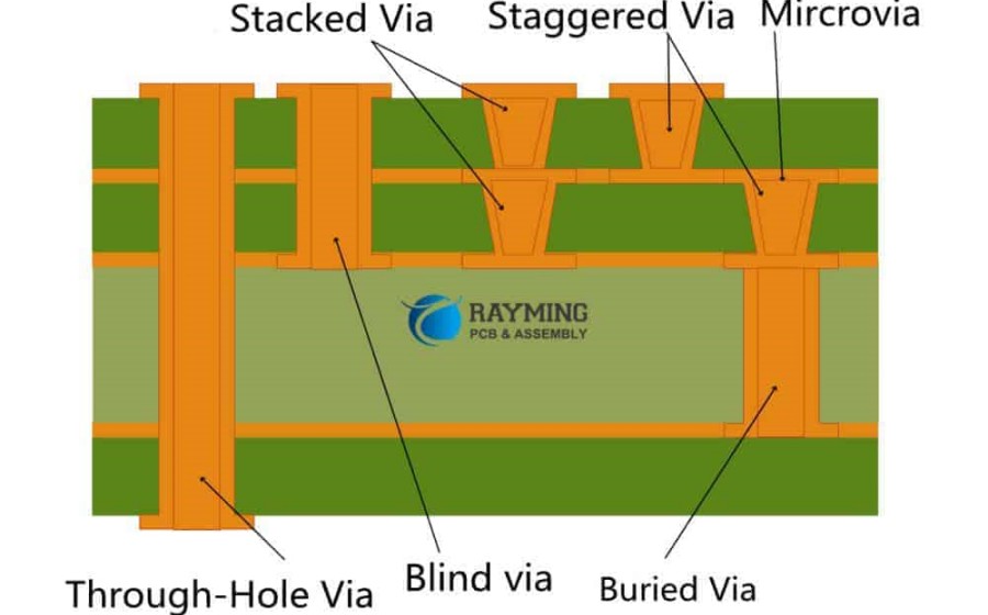
What are Blind Vias?
Blind vias are holes drilled in a PCB that are plated to connect only between some of the layers, rather than connecting all the way from the top layer to the bottom layer. In a 4 layer board, common blind via configurations include:
- Connecting Layers 1 and 2
- Connecting Layers 2 and 3
- Connecting Layers 3 and 4
Blind vias stop at the first copper layer encountered when drilling and do not extend all the way through the PCB stackup. They enable interconnections between internal layers without occupying space on the outer layers.
Advantages of Blind Vias
Compared to through vias, blind vias offer several key benefits:
- Higher routing density: Since blind vias do not require pad stacks on the outer layers, more space is available for routing signals on the top and bottom layers.
- Signal isolation: Signals can be contained within layers by using contained blind vias, reducing noise coupling between layers.
- Layer count reduction: By utilizing blind and buried vias, some designs can eliminate entire signal layers compared to an equivalent board using only through vias.
- Improved impedance control: With no stub created, blind vias allow for more consistent impedance especially for high-speed signals.
4 Layer PCB Stackup Configurations
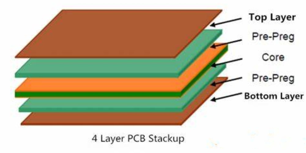
To understand where blind vias are used in a 4 layer board, we first need to cover the most common layer stackup configurations. Here are three typical arrangements:
1. Signal-Power-Signal-Power
This stackup has a signal routing layer on Layers 1 and 3, with a power plane on Layers 2 and 4:
Copy code
Layer 1: Signal Layer 2: Power Layer 3: Signal Layer 4: Power
Blind vias would be used to connect Layers 1 and 2 for power connections to the Layer 2 plane. And Layers 3 and 4 would be connected similarly.
2. Signal-Signal-Power-Power
In this stackup, the signal layers are together in the middle, with power planes on the outer layers:
Copy code
Layer 1: Power Layer 2: Signal Layer 3: Signal Layer 4: Power
Blind vias connect Layers 2 and 3 for signal routing between the layers. And Layers 1 and 2 or Layers 3 and 4 are connected for power.
3. Power-Signal-Signal-Power
Here the signal layers are separated by power planes:
Copy code
Layer 1: Power Layer 2: Signal Layer 3: Signal Layer 4: Power
Blind vias connect Layers 1 and 2, Layers 2 and 3 for signal routing, and Layers 3 and 4. This provides excellent isolation between the signal layers.
Manufacturing Process for 4 Layer Blind Vias
Fabricating a PCB with blind vias requires advanced drilling and plating processes compared to a simple through-hole board. Here are the key manufacturing steps:
1. Drilling
Blind vias are typically drilled one layer at a time, often with multiple drill bits. For a 4 layer board:
- First, standard through holes are drilled from Layer 1 through Layer 4.
- Next, Layer 1 is used as the drill stop layer to create vias connecting Layers 2 and 3.
- Finally, Layer 3 serves as the stop when drilling Layer 1 to Layer 2 and Layer 3 to Layer 4 blind vias.
This sequential process allows each blind via depth to be precisely controlled.
2. Desmear and Plating
After drilling, a desmear process removes any resin smear from the hole walls created during drilling. This prepares the holes for metallization.
Blind vias are then plated with an electroless copper process, followed by electroplating to build up the desired copper thickness. Plating connects the layers associated with each blind via.
3. Outer Layer Processing
Additional steps are performed to create the traces and features on the outer layers (Layer 1 and Layer 4). This includes photoimageable processing, copper etching, outer layer hole punches, and soldermask application.
4. Final Finish
The final PCB then goes through inspection, cleaning, and whatever finish is specified (ENIG, immersion tin, etc). The result is a high-quality and reliable 4 layer PCB with plated blind vias.
Key Applications of 4 Layer Blind Vias
Some of the most common applications that utilize blind vias in 4 layer boards include:
High Speed Digital Designs
Blind vias allow high-speed signals like DDR memory buses to be routed on inner layers with minimal stub effects. The lack of stubs helps maintain signal integrity. Containing signals internally also reduces EMI.
RF and Analog Circuits
In RF designs, blind vias allow ground planes to be placed close to signals to achieve controlled impedance across multiple layers. For analog, sensitive signals can be isolated on inner layers.
Tight-Pitch BGAs
Using blind and buried vias under BGA packages maximizes routing space available on the outer layers. More routing channels allows escape routing from tight BGA pitches.
LED Circuit Boards
LED PCBs frequently use blind/buried vias to connect inner layers under dense LED arrays while keeping the solder-side clear of vias.
Reducing Layer Count
Careful use of blind/buried vias may eliminate the need for entire signal routing layers in some designs. This lowers costs.
Mixed-Signal Boards
Blind vias isolate digital and analog signals by containing them within layers. Digital signals can also be sandwiched between ground planes.
Guidelines for 4 Layer Blind Vias
Here are some key guidelines to follow when working with blind vias in 4 layer PCBs:
- Minimize the total number of blind via barrels. Each one adds cost.
- Maximize the drill ratio relative to final hole size for reliability.
- Tent vias whenever possible, especially over plane layers.
- Avoid overlapping or adjacent blind via pads whenever feasible.
- Use larger capture pads for blind vias for improved hole tolerances.
- Verify blind/buried layer connectivity in layout before manufacture.
Pros and Cons of 4 Layer Blind Vias
Let’s examine the relative advantages and disadvantages of using blind vias compared to through-hole vias in 4 layer boards:
Pros
- Increased routing density from eliminating through-hole pad stacks
- Lower layer counts possible in some designs
- Reduced stub effects on high-speed signals
- Containing signals reduces crosstalk and EMI
- Planes can be placed just below or above signals
- Easier impedance control compared to through vias
Cons
- Increased manufacturing time and cost
- Requires advanced PCB fab capability and equipment
- Blind via reliability may be reduced vs through vias
- More difficult rework of blind vias
- Requires careful layer planning for signal isolation
Summary
To summarize, 4 layer PCBs with blind vias provide performance, routing, and isolation benefits compared to relying solely on through-hole vias between all layers. Blind vias are essential in many high-speed, high-density, and mixed-signal designs to maximize routability and signal integrity.
However, using blind vias also introduces additional fabrication complexity and cost. Careful planning is required to utilize blind vias effectively while minimizing negative impacts on manufacturability, especially for low volume or prototype boards.
Frequently Asked Questions
What is the minimum board thickness for 4 layer blind vias?
The minimum thickness for a reliable 4 layer PCB with 3 mil finished blind vias is around 60 mils, although 62-64 mils is recommended. Thinner boards are possible but may have reduced via reliability and structural integrity.
Can I have blind vias in a 2 layer board?
No, blind vias require 3 or more board layers, since they connect internal layers without going through the entire board. In a 2 layer board, all drilled holes are through vias.
Should I use blind or buried vias in 4 layer boards?
Blind vias are generally preferable to buried vias in 4 layer designs. Buried vias connect internal layers without reaching either the top or bottom layer, making them difficult to inspect and rework. Blind vias connect one internal layer to an outer layer.
How do I indicate blind vias in my PCB design?
In your CAD and layout software, you specify blind vias by selecting the start and stop layers for the via. Your PCB fab will also have stackup and netlist requirements. Consult their guidelines.
Can microvias be combined with blind vias?
Yes, you can incorporate microvias (smaller laser drilled vias) along with mechanically drilled blind vias for increased connection density. This does further increase fabrication complexity however.


Leave a Reply