Introduction
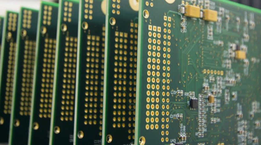
High density interconnect (HDI) printed circuit boards (PCBs) have become increasingly popular in recent years due to the growing demand for more compact and complex circuit designs. 28 layer HDI PCBs represent the cutting edge of PCB technology, packing intricate circuitry and components into an extremely dense configuration. Choosing the right 28 layer HDI PCB manufacturer is crucial to ensure your boards are produced reliably and to the highest standards. This article provides an in-depth look at what to consider when selecting a 28 layer HDI PCB manufacturing partner.
What is a 28 Layer HDI PCB?
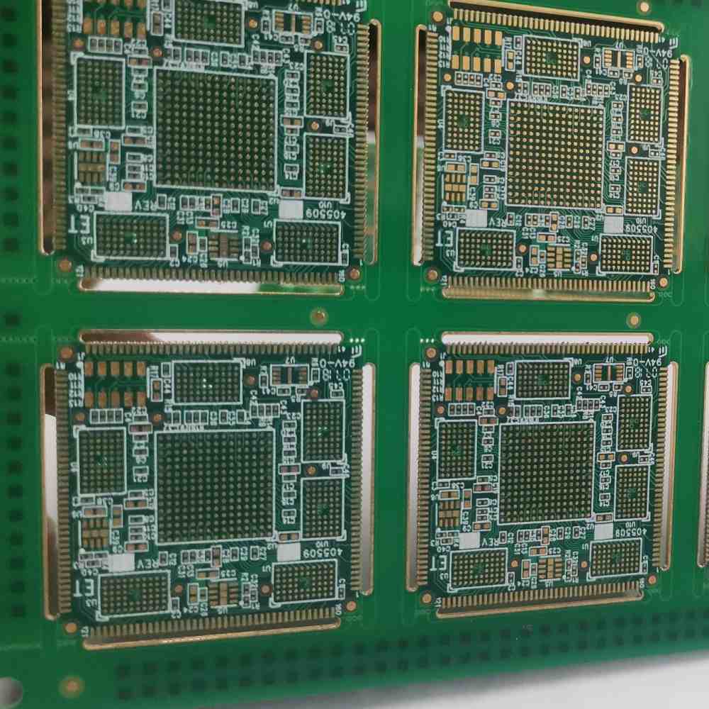
HDI PCBs use microvias and thin dielectric layers to enable higher component densities compared to conventional PCBs. They allow circuits to be packed more tightly together, reducing the overall footprint of the board. 28 layer HDI boards interweave 28 conductive copper layers separated by dielectric insulating substrates.
Here are some key features of 28 layer HDI PCBs:
- Extremely dense circuitry: Up to 28 conductive layers are stacked together, connected using microvias. This enables far higher component density than conventional PCBs.
- Thin dielectric layers: The insulating dielectric layers separating the copper layers are extremely thin, some as low as 3-4 microns. This allows tight stacking of conductive layers.
- Microvias: Small vias with diameters under 150 microns are used to connect layers rather than through-hole vias. This further increases circuit density.
- Fine line/space: Line width and spacing down to 15 microns or below is typical. Allows for intricate circuit traces.
- High frequency: Their noise reduction and impedance control capabilities make them suitable for high frequency applications like 5G.
- Miniaturization: 28 layer HDI PCBs facilitate miniaturization of electronics due to their high component density.
Challenges of 28 Layer HDI PCBs
While offering many benefits, 28 layer HDI PCBs also pose some manufacturing challenges:
- Extreme precision required: With traces and spaces less than 20 microns, highly precise manufacturing is essential. This requires advanced equipment and processes.
- Tight layer alignment: Aligning 28 layers accurately during lamination requires specialized equipment and experience. Misalignment can lead to defects.
- Thin dielectric control: Controlling dielectric thickness uniformly at 3-4 microns is challenging and vital to performance.
- Microvia reliability: Ensuring reliable connections with microvias under high density requires expertise.
- Thermal management: Dense circuitry leads to thermal buildup which must be mitigated through design and manufacturing optimization.
- Testing: Verifying the integrity of traces across 28 layers requires advanced testing capabilities.
Key Considerations for 28 Layer HDI PCB Manufacturers
Technology and Equipment
Manufacturing 28 layer HDI PCBs requires state-of-the-art fabrication technology and equipment. Key capabilities to look for include:
- Direct imaging systems: This laser lithography system can create micro-scale traces and spaces. Unlike traditional photolithography, it eliminates the need for films.
- High-density interconnect (HDI) lamination presses: Using advanced vacuum and heating technology, these presses laminate together thin dielectric layers accurately.
- Microvia formation: Laser, plasma, or photolithographic processes should be capable of producing reliable microvias under 100 microns in diameter.
- X-Ray drilling: For forming high-ratio depth microvias.
- Automatic optical inspection (AOI): Detects microscopic defects during fabrication using advanced optics and imaging.
- Impedance testing: Measures impedance across all layers to dial in performance, especially for high-speed boards.
- Microsectioning: Allows cross-sectional analysis of boards to inspect layer alignment, microvia formation, and other internal features.
Experience
Look for manufacturers with experience specifically producing cutting-edge HDI PCBs in volume. They should have expertise across the entire manufacturing process from design to inspection and testing. Deep know-how with advanced HDI materials, fabrication processes, and handling is key.
Quality Systems
Rigorous quality control is crucial when working at micro-scale dimensions. Manufacturers should be certified to the latest quality standards:
- ISO 9001:2015 – Sets standards for quality management systems.
- IPC Class 3 – Refers to stringent standards for HDI PCB fabrication and quality acceptance.
- IATF 16949 – The highest automotive industry quality standard.
Ask about their quality procedures like process controls, inspection steps, qualifications, and more. They should also have safeguards against counterfeiting including laminate and component traceability.
Customer Service
The PCB manufacturer should assign dedicated engineering support contacts to help optimize designs for their process capabilities. They should be responsive and willing to collaborate iteratively to refine the design and process as needed.
Top 28 Layer HDI PCB Manufacturers
Many PCB manufacturers offer conventional multilayer boards, but far fewer have the advanced expertise and capabilities necessary for 28 layer HDI boards specifically. Here are some of the top manufacturers known for high-layer count HDI PCB production:
TTM Technologies
TTM Technologies is one of the world’s largest PCB producers with advanced HDI technology. Some of their capabilities include:
- 30+ HDI layers
- Line/space down to 15/15μm
- Microvias from 75μm
- 0.6mm pitch flip chip
- 400mm x 300mm panel size
They utilize an innovative semi-additive process (mSAP) for HDI fabrication and have expertise working with RF/microwave and flex-rigid designs.
AT&S
AT&S is an Austrian company that is one of Europe’s largest PCB manufacturers. For advanced HDI they offer:
- Up to 30 conductive layers
- Line/space down to 10/10 μm
- Microvias from 60 μm
- 0.4 mm pitch flip chip
Their process expertise includes build-up, stacked, and flex-rigid boards. They also do in-house HDI design and simulation services.
Compeq
Compeq specializes in HDI boards and was one of the earliest manufacturers to achieve under 15μm line/space capabilities. They have:
- Up to 36 build-up layers
- Line/space down to 10/10 μm
- 0.3mm pitch flip chip
- Microvias from 25 μm
Compeq provides both conventional and additive processing. They target telecom, automotive, and advanced packaging.
Tripod Technology
Tripod offers specialized processing and quality control for high layer count HDI up to 20 layers. Their credentials include:
- Line/space down to 8/8 μm
- Microvias from 60 μm
- 16-layer MLBs
They focus on HDI technology integration and are certified to multiple quality standards including ISO and IATF 16949.
Unimicron
Unimicron fabricates advanced PCBs for IC substrates and HDI applications. They have:
- Up to 36 conductive layers
- Line/space down to 15 μm
- Microvias from 40 μm
- Panel sizes up to 510mm x 510mm
They are experienced in stacked microvia and fine line space HDI. Unimicron also offers HDI design services and quick-turn fabrication.
Key Questions to Ask Manufacturers
When vetting 28 layer HDI PCB manufacturers, here are some important questions to ask:
- What is your maximum achievable layer count and minimum line/space?
- What advanced PCB technologies like microvias, stacked vias, etc. do you offer?
- What HDI materials are you qualified to process? What dielectric thicknesses?
- Do you allow factory tours or process audits? Can you share internal testing data?
- What quality certifications do your factories/processes have?
- What statistical process control and quality procedures are used?
- Do you have dedicated HDI engineering support for design reviews and collaboration?
- How do you ensure raw material traceability and counterfeit avoidance?
- What test and inspection capabilities do you have for verifying HDI board quality?
- Do you have expertise producing similar complex HDI boards in volume for demanding industries?
- How quickly can you turn around HDI prototypes for evaluation?
- What design, simulation, and DFM support services are available?
Getting detailed answers to these questions will help qualify an HDI manufacturer’s true capabilities and expertise.
28 Layer HDI PCB Design Considerations

While the PCB manufacturer handles fabrication, the designer plays a crucial role in optimizing boards for manufacturability and reliability. Here are some key design practices:
Board Stackup
- Use thinner dielectrics to maximize layer count, but ensure uniform thickness.
- Stack microvia layers adjacent to each other when possible.
- Place high speed layers close to the board center for optimal signal integrity.
- Ensure adequate ground plane layers for controlled impedance.
Component Layout
- Leave adequate keep-out zones around high pin count components for routing space.
- Group components with high interconnectivity near each other.
- Ensure components align with BGA grids properly.
- Give adequate clearance between tall components to allow lamination.
Microvia Design
- Connect microvias in a daisy chain rather than stub connections when possible.
- Stagger adjacent microvias to avoid weakening dielectrics.
- Limit aspect ratios to around 1:1 where possible.
- Avoid placing microvias under BGA pads, use adjacent pads if needed.
Thermal Management
- Use thermal core and plate designs to dissipate heat from high power areas.
- Place heat generating components over thermal vias where possible.
- Leave gaps in ground planes for low-loss lateral heat conduction.
- Use wide copper planes for heat spreading from hot spots.
Following sound design practices and collaborating closely with the PCB manufacturer will yield the best results. Designers should leverage the manufacturer’s expertise early in the process.
Conclusion
28 layer HDI PCBs enable innovators to pack more performance into ever smaller electronics. But realizing these complex boards requires world-class manufacturing expertise spanning advanced processes, equipment, quality systems, and experience. Finding the right partner ensures your cutting-edge products are produced reliably at scale. This guide covers key considerations for selecting a 28 layer HDI PCB manufacturing partner capable of delivering on the promise of this exciting technology. With diligent vetting using the criteria outlined, you can feel confident entrusting your most advanced designs to production.
Frequently Asked Questions
What are some leading industries using 28 layer HDI PCBs?
Some of the industries driving adoption of 28 layer HDI PCBs include:
- Telecommunications – 5G infrastructure relies on advanced PCBs.
- Automotive – Autonomous driving requires ever more complex circuits.
- Aerospace and defense – Miniaturization of avionics and electronics.
- Consumer electronics – Packing more computing power into small form factors.
- Medical – Implants and miniature instruments.
Are there environmental concerns around 28 layer PCB manufacturing?
Yes, the chemicals and materials involved in fabricating multilayer PCBs raise environmental considerations including:
- Chemical handling and waste – Proper precautions must be taken.
- Flame retardants – Brominated flame retardants are sometimes used in PCBs but being phased out due to toxicity concerns.
- Metal extraction – Resources like copper and gold are used in PCB fabrication.
- Recycling – Reclaiming metals and materials from electronics at end of life is important.
Leading PCB manufacturers implement clean production initiatives to mitigate environmental impacts. Choosing suppliers with good environmental records is recommended.
How are microvias formed in HDI PCBs?
There are three primary methods of forming microvias in HDI PCB fabrication:
Laser – A CO2 laser ablates the dielectric material to form a via. This is the most widespread method.
Plasma – Oxygen plasma selectively etches dielectric to create vias. Allows small diameters.
Photovia – Photolithographic patterning followed by etching creates microvias. Tight process control is required.
Manufacturers often use a combination of these processes depending on the via size, layer, and other requirements.
What new PCB technologies are emerging beyond HDI?
Some emerging PCB fabrication technologies on the horizon include:
- Embedded actives – Integrating active components like capacitors and resistors directly into the PCB layers.
- Flexible electronics – Boards fabricated on thin, flexible plastic substrates.
- Stretchable circuits – Conductors screen printed on elastic materials.
- Chip packaging – Manufacturing techniques adapted to integrate circuits directly into packages.
- 3D printing – Additive fabrication techniques under development for electronics.
- Smart PCBs – Boards with integrated sensing, processing, and acting capabilities.
How can I get started designing 28 layer HDI PCBs?
Here are some tips for designing your first 28 layer HDI PCB:
- Learn the constraints of your manufacturer’s capabilities – line widths, microvia sizes, etc.
- Start with simpler layer counts and work your way up in complexity as you gain experience.
- Leverage your manufacturer’s design resources for feedback and guidance.
- Use a PCB design software like Cadence Allegro with advanced HDI features.
- Employ proper stackup arrangements, component layouts, and routing strategies.
- Build in design margin on trace spacing and dielectric thicknesses.
- Create a detailed design specification document.
- Work iteratively with engineering prototypes before full production.


Leave a Reply