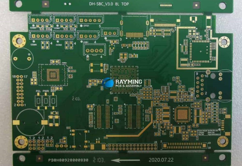
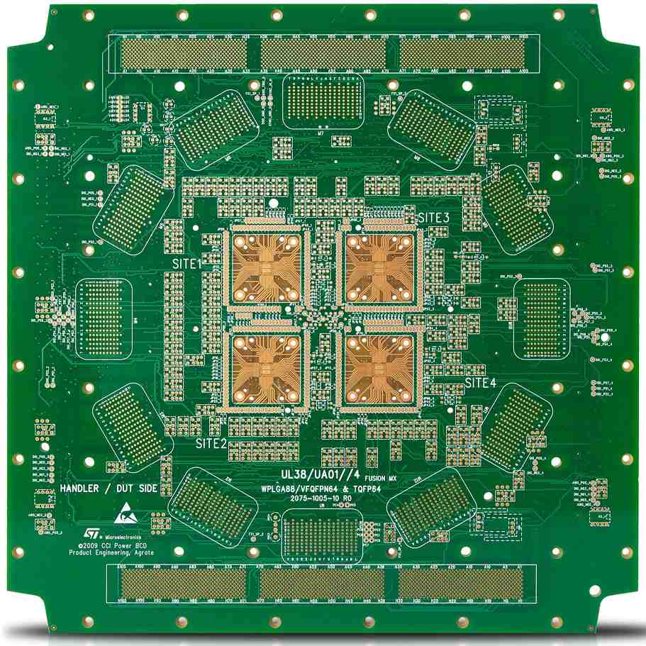
As printed circuit boards (PCBs) become increasingly complex, manufacturers require advanced capabilities to produce high-density interconnect (HDI) boards with many layers. 26 layer HDI PCBs represent the leading edge of PCB technology, packing intricate circuitry into an extremely compact space.
Selecting the right 26 layer HDI PCB manufacturer is crucial to ensure your boards meet quality, reliability and performance requirements. This guide provides a comprehensive overview of 26 layer HDI manufacturing, including key manufacturer capabilities, quality control processes, and factors to consider when choosing a partner.
HDI PCBs: Enabling Complex, High-Density Designs
HDI refers to technology that allows routing of traces and vias on PCBs with a higher density than conventional PCBs. This enables more complex circuit designs in a smaller space.
Key characteristics of HDI PCBs:
- Trace/space width and via pad size of 6 mils or less
- Stacked microvias with 6 mil diameter or less
- Thin dielectric layers, typically 3 mils or less
- More than six conductive layers
With 26 layers, HDI PCBs maximize circuit density. They utilize advanced manufacturing techniques to layer intricately routed traces and components within an extremely compact area.
HDI capabilities make high layer count PCBs ideal for products like:
- Smartphones
- Wearable devices
- Internet of Things (IoT) devices
- Advanced driver assistance systems (ADAS)
- Medical devices
- Aerospace and defense electronics
In short, 26 layer HDI PCBs provide the interconnectivity needed for the most complex and compact modern circuit designs.
Key Capabilities for 26 Layer HDI PCB Fabrication

Producing 26 layer HDI PCBs requires robust design engineering expertise tightly integrated with advanced manufacturing capabilities. Here are some of the essential competencies for 26 layer HDI PCB production:
HDI Design Engineering
The design phase lays the groundwork for manufacturing. HDI design expertise includes:
- Board stackup design: Determining layer composition, materials, thickness and sequence for optimal HDI performance. This includes decisions on number of laminated cores versus built-up dielectrics.
- Trace/space engineering: Optimizing line width, space width and via sizes, integrated with layer stackup, to meet circuit density and performance requirements.
- Matched impedance design: Managing impedance across layers, critical for high speed signals.
- Signal integrity analysis: Using modeling and simulation to predict electrical performance and prevent issues like crosstalk.
- DFM guidance: Providing design for manufacturability (DFM) feedback to ensure designs are producible.
Photolithography
Photolithography patterns the intricate circuitry onto each conductive layer. Key capabilities include:
- Laser direct imaging (LDI): Laser plotters directly expose fine features onto photoresist coated layers. Far superior to older mask-based methods.
- High resolution: LDI systems with 5 micron resolution or better are standard. 1 micron resolution is preferred for microvias.
- Advanced resists: Thinner resists enabling tighter trace/space. Lead-free compatible resists required.
- Automated optical inspection (AOI): AOI after lithography identifies defects for correction before plating.
Plating Processes
Plating deposits the copper traces and fills microvias:
- Copper electroplating: Dense, uniform copper electroplating is essential for even trace formation.
- Microvia fill: Specialized copper overplating fills microvias reliably without voids.
- Surface finishes: Electroless nickel immersion gold (ENIG), organic solderability preservative (OSP), and other finishes.
Laser Drilling
Lasers drill tiny vias through layers:
- Blind and buried vias: Achieve vertical interconnections between internal layers.
- High density microvias: 6 mil diameter vias or smaller; 8-10 mils on densely packed grid.
- Depth control: Precise depth control for blind/buried vias.
- Tapered vias: Create optimized taper for adequate resin fill.
Layer Alignment and Registration
- Layer-to-layer registration: Tight alignment of layers, especially critical for microvias and impedance control. Usually achieved with laser or optical registration.
- Automated optical inspection (AOI): Inspect layer alignment and identify any registration issues.
Complex Circuit Integration
- Sequential lamination: Build up dielectric layers with advanced sequential lamination techniques.
- Via in pad (VIP): Enable connections through pads for increased routing in tight spaces.
- Embedded components: Embed capacitors, resistors and other components within layers.
- Flex/rigid flex: Combine rigid multilayer with flexible circuits.
- 3D interconnects: Laser-drilled mechanical vias allow vertical interconnections or connections between board surfaces.
Testing and Inspection
Extensive testing ensures reliability:
- In-circuit test (ICT) checks continuity, shorts, and opens after fabrication.
- Automated optical inspection (AOI) throughout the process.
- X-Ray inspection of microvias and through-holes. Checks for fill defects like pinholes.
- Cross-section analysis verifies trace geometries, resin fill, layer alignment under microscope.
- Electrical testing such as flying probe tests.
- Impedance testing, for controlled impedance boards.
- Ionic contamination testing
Quality Management Standards for 26 Layer HDI Manufacturing
Reputable 26 layer HDI PCB manufacturers will hold the following major quality certifications:
- IPC 6012 Class 3 certification for HDI manufacturing rigor
- ISO 9001 certification for quality management systems
- IPC-A-600 acceptability standard for workmanship
- AS9100 aerospace standard for high reliability
- ITAR registration for defense customers
They also implement best practices including:
- Statistical process control (SPC) – Analysis and monitoring of processes to eliminate variability
- FOD (foreign object debris) control – Vigilant prevention of contaminants
- ESD (electrostatic discharge) control – Protection of ESD-sensitive components and materials
- CAM/CAD data integrity – Secure workflows for design data translation to manufacturing
- Traceability – Part marking standards and serialization for full traceability
- Change management – Strict change control to prevent unauthorized modifications
- Continual improvement – Kaizen, 5S, Lean and other methods to improve productivity, quality and reduce waste
Together, these certifications, controls and best practices enable 26 layer HDI PCB production with the highest reliability and consistency.
Choosing a 26 Layer HDI PCB Manufacturer
With 26 layer HDI PCBs representing the leading edge of printed circuit board technology, you need an expert manufacturing partner. Here are key factors to evaluate:
Extensive HDI Experience
Look for manufacturers with at least 10 years of experience producing multilayer HDI boards at high volumes. They should have expertise across the full range of HDI design density, layer counts and interconnect complexities.
Leading Edge Capabilities
Evaluate engineering depth, site equipment and certifications. Look for capabilities like 1 micron lithography, sequential lamination, laser drilling to 5 mils, 10+ AOI systems, microsectioning and impedance testing.
Rigorous Quality Systems
As described earlier, choose a partner holding multiple stringent quality certifications backed by statistical process control, automation and proven best practices.
Vertical Integration
Fully integrated manufacturers control more of the process for quality and security. Audit their capabilities across design, fabrication, assembly, test and inspection.
Customer Focus
The right partner understands your goals, requirements and product roadmap. They add value through collaboration, DFM guidance, and process innovation tailored to your needs.
Competitive Pricing
With advanced automation and economies of scale, leading HDI manufacturers offer cost-competitive pricing, passing savings to customers. Avoid partners lacking scale or capabilities that inflate costs.
Conclusion
As products require advanced connectivity in extremely constrained spaces, 26 layer HDI PCBs provide the interconnect solution. Leading HDI PCB manufacturers offer the complete expertise and capabilities to fabricate these boards reliably and cost-effectively. Choosing the right partner levels up your supply chain to meet the needs of the most sophisticated electronics.
26 Layer HDI PCB Manufacturing FAQ
Here are answers to some frequently asked questions about manufacturing 26 layer HDI PCBs:
Q: What are typical construction techniques for 26 layer HDI boards?
A: A 26 layer board will typically consist of multiple 4-8 layer core panels that are laminated together into a single circuitized structure. High layer count boards generally use a combination of core and build-up construction to optimize cost and performance.
Q: What are recommended dielectric materials for 26 layer HDI boards?
A: Common dielectrics include FR-4, polyimides, PTFE composites, and low-loss thermoset or thermoplastic materials. Material choice depends on electrical and mechanical requirements. Polyimides excel for flexibility while PTFE has superb electrical properties.
Q: What design elements help maximize routability in 26 layer HDI designs?
A: Use of microvias is critical – these provide connections between layers using minimal space. Stacked microvias, skip vias and back-drilled vias further optimize routing density. Blind and buried vias are heavily used. Liberal use of grounded planes between signal layers reduces crosstalk.
Q: What are some key testing methods used to validate 26 layer HDI board quality?
A: Electrical testing validates continuity, shorts and opens. Automated optical inspection (AOI) checks trace geometries. X-ray inspects proper microvia fill. Microsectioning confirms layer alignment, plating quality and dielectric fill under high magnification. Impedance testing validates matched impedance on controlled impedance designs.
Q: What design and specification elements are most critical for 26 layer HDI designs?
A: Trace routing, layer stackup, impedance control and material selection are critical in design. Key specifications include trace/space width, microvia size and spacing, hole wall tolerances, and dielectric properties. Close collaboration between designer and manufacturer ensures achievability.


Leave a Reply