Introduction
High density interconnect (HDI) PCBs have become increasingly popular in recent years due to the demand for smaller and more complex circuit designs in industries like consumer electronics, telecommunications, aerospace and defense. HDI PCBs allow for finer lines and spaces, smaller vias, and higher connection densities compared to conventional PCBs. This enables greater circuit complexity, more compact design, and improved electrical performance.
22 layer HDI PCBs represent some of the most advanced and complex PCB solutions available today. They enable extremely high component densities and very efficient routing for space-constrained and high-speed designs. However, manufacturing these boards requires specialized expertise and advanced equipment. In this article, we will look at what 22 layer HDI PCBs are, their benefits and applications, and what to look for in a qualified 22 layer HDI PCB manufacturer.
What are 22 Layer HDI PCBs?
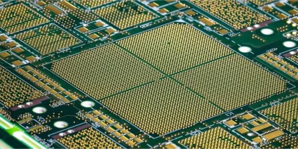
HDI PCBs use microvias to interconnect layers, rather than through holes like conventional multilayer PCBs. This allows multiple circuit layers to be stacked closely together, without requiring as much surface area for interconnections. 22 layer HDI boards contain even more circuit layers than typical HDI boards.
Here are some key characteristics of 22 layer HDI PCBs:
- Total layer count – 22 layers, including 20+ circuit layers
- Line width/spacing – As small as 2/2 mils (0.05 mm)
- Microvia diameters – As small as 0.005 inches (0.127 mm)
- Dielectric thickness – Thinned dielectrics around 0.5 to 0.75 mils per layer
- High circuit density – More than 300,000 holes per square meter
The microvias and thin dielectrics allow the circuit layers to be stacked very closely together. This provides space for routing complex circuits but in a smaller physical footprint. The high density of microvias enables extensive interconnections between layers.
Benefits and Applications of 22 Layer HDI PCBs
The ultra-high interconnect density and small features of 22 layer HDI PCBs provide a number of important benefits for advanced designs:
Smaller size – The compact stacking of circuit layers allows very complex boards to fit into tight spaces. This is critical for portable and space-constrained electronics.
Higher speeds – Thin dielectrics between layers reduce capacitance for improved high-speed signal integrity. Shorter traces also minimize delays.
Lower weight – HDI technology minimizes the amount of insulating material required between layers, resulting in a lighter board. This is advantageous for portable devices as well as aerospace applications.
Noise reduction – Careful control of dielectric thickness and board materials results in lower noise. This helps maintain signal integrity at high frequencies.
Reliability – Microvias have lower stresses than plated through holes. This improves reliability and prevents cracks from developing.
Design flexibility – The use of blind and buried vias enables greater routing flexibility by allowing connections between non-adjacent layers.
Some of the most common applications for 22 layer HDI PCBs include:
- Smartphones, tablets, and wearable electronics
- High density computer servers and data centers
- Networking and telecom equipment like routers and switches
- Advanced radar, guidance systems, and avionics
- Medical imaging equipment
Any product where complexity, high speeds, small size, and lightweight are critical can benefit from utilizing 22 layer HDI PCB technology. The boards provide the interconnect density necessary for shrinking electronic packages with rising functionality demands.
22 Layer HDI PCB Manufacturing Capabilities
Producing reliable 22 layer HDI PCBs requires an extremely capable manufacturing workflow featuring state-of-the-art processes, equipment, and quality control. Here are some key capabilities to look for in a PCB manufacturer:
Fine line production – Manufacturing PCBs with 2 mil lines/spaces requires specialized photolithography equipment and very tight process control. This includes proper film etching, precise lamination, and excellent metal deposition.
Advanced drilling – Drilling high numbers of small microvias calls for high precision drilling machines and bits. Tight drill position accuracy and hole wall quality help enable plating of small microvias.
Thin core handling – Thin dielectric core materials around 0.5 mils are prone to warping and wrinkling. The manufacturer must have effective handling procedures to prevent damage during inner layer preparation.
Alignment accuracy – Aligning layers with registration accuracy around 2 microns or better is critical for reliable interconnections between layers.
Plating capabilities – The numerous microvias must be plated with copper to connect layers electrically. High throwing power plating is needed to properly plate into tiny vias.
Solder mask process – Tight resolutions are required to accurately define openings in the solder mask for such small features. The walls should also be clean for component mounting.
Testing and inspection – Testing functionality at GHz speeds requires specialized flying probe or fixture testing. Automated optical inspection (AOI) is also important for verifying acceptable board quality.
Not all PCB manufacturers can reliably produce boards at 22 layer HDI complexity. Partnering with a shop that has proven expertise and credentials in manufacturing advanced HDI designs is highly recommended.
How to Choose a Great 22 Layer HDI PCB Manufacturer
Here are some of the key factors to consider when selecting a 22 layer HDI PCB manufacturer:
Experience with complex HDI – Look for years of experience manufacturing 10+ layer HDI boards at high volumes. Proven capability with multiple HDI projects is ideal.
Tight quality controls – The manufacturer should adhere to IPC standards and have quality certifications like ISO 9001. They should inspect rigorously and replace any defective materials.
Engineering support – To fabricate complex boards reliably requires engineering collaboration between your team and the manufacturer. They should review designs for manufacturability and provide helpful feedback.
Feedback and responsiveness – Good communication is crucial for high-mix, low-volume complex boards. Ensure they provide regular project status updates and are responsive if any issues arise.
Proximity and security – For sensitive defense or communications projects, you may prefer a domestic PCB manufacturer with on-shore production facilities. Proximity can also aid engineering collaboration.
Equipment and capabilities – Examine their equipment list and facility details. Look for leading edge fabrication equipment and demonstrated capabilities matching your needs.
Third party verification – Independent audits like UL or IPC certifications help validate manufacturing processes and quality management. Site visits to audit their facility may also help qualify vendors.
By selecting a reliable 22 layer HDI PCB manufacturing partner, you gain the assurance that your boards will be fabricated correctly and deliver the required functionality for your product designs. Careful vetting of manufacturers upfront prevents potential issues during volume production.
Frequently Asked Questions about 22 Layer HDI PCB Manufacturing
Here are answers to some common questions about procuring 22 layer HDI PCBs:
How long does manufacturing 22 layer HDI PCBs typically take?
For prototype quantities, allow 3 to 4 weeks total production time once design files are approved. For higher volumes, multipanel designs can reduce costs and time.
What design considerations are important for these boards?
Use impedance controlled routing for critical signals. Plan carefully for thermal management with minimal copper at layer transitions. Be diligent about meeting minimum annular ring requirements around microvias.
What are the typical lead times for production orders?
Once the design is finalized, verified boards can usually ship within 2 weeks. Lead times for initial volumes may extend to 4-6 weeks for rigorous quality assurance testing.
How should 22 layer HDI PCBs be handled and processed?
Ensure proper ESD control procedures. Use special care during depaneling, assembly, and rework to prevent damage given the thin cores. Clean regularly to prevent problems at small features.
What testing should be conducted to verify quality?
At minimum, electrically test 100% of nets for opens/shorts with flying probe test. Implement ICT and AOI inspection at multiple fabrication steps. Perform cross-sectioning periodically.
Conclusion
22 layer HDI PCB technology enables highly complex yet miniaturized printed circuit board designs featuring very fine lines and ultra-dense interconnects. These specialty boards require rigorous design expertise and advanced manufacturing capabilities to produce reliably. By partnering with an experienced, well-equipped PCB manufacturer, you can leverage 22 layer HDI PCBs to meet the needs of your sophisticated electronics projects while minimizing development and fabrication risks. Carefully qualifying your chosen manufacturer will pay dividends over the long term through superior quality boards delivered consistently on schedule.


Leave a Reply