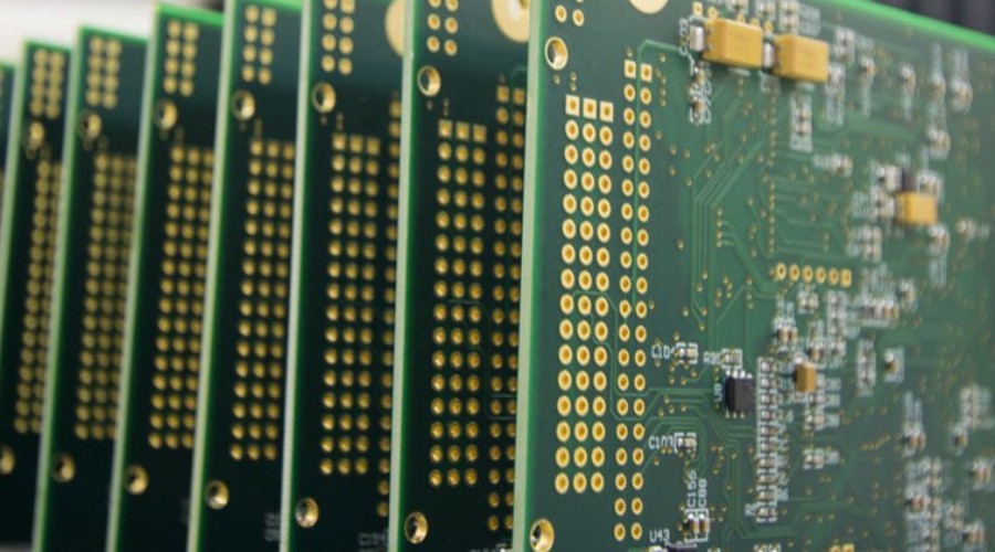
Theprinted circuit board (PCB) industry is constantly evolving to meet the needs of increasingly complex and compact electronic devices. One area that has seen significant innovation in recent years is high-density interconnect (HDI) PCBs. HDI technology allows for tighter spacing between traces and vias, enabling more circuitry to be packed into the same footprint area. The continuing drive toward miniaturization and functionality has now led to the development of 20 layer HDI boards.
What are HDI Boards?
HDI stands for high-density interconnect. HDI PCBs use very fine lines and spaces to increase the routing density compared to conventional PCBs. This allows HDI boards to accommodate more high-speed signals and components in the same area.
Some key characteristics of HDI boards:
- Trace widths and spacings under 6 mils
- Microvias with diameters 6 mils or under
- More than 4 routing layers
- Often employ build-up construction
- Typically use thicker copper layers (1 oz or greater)
HDI technology enables routing traces between closely spaced surface mount components. It is essential for many modern compact consumer electronics.
Advantages of 20 Layer HDI Boards

Increasing the layer count allows 20 layer HDI boards to offer even greater routing density and performance benefits:
- Accommodate extremely complex circuitry and component density
- Enable high-speed signal integrity across more layers
- Facilitate heavily partitioned power delivery networks
- Provide enhanced EMI shielding and isolation between circuits
- Allow for more power and ground planes to reduce impedances
With 20 routing layers, these boards can incorporate many high-speed signals and components without compromising performance. The numerous power and ground planes also enhance power integrity.
Here is a comparison of key specs between standard HDI and 20 layer HDI boards:
| Spec | Standard HDI | 20 Layer HDI |
|---|---|---|
| Max Traces Spacing | 4-6 mils | 2-4 mils |
| Number of Routing Layers | 6-12 | Up to 20 |
| Microvia Size | 6-8 mils | 4-6 mils |
| Microvia Pad Size | 8-12 mils | 6-8 mils |
| Line Width | 6-8 mils | 4-6 mils |
| Line Spacing | 6-8 mils | 4-6 mils |
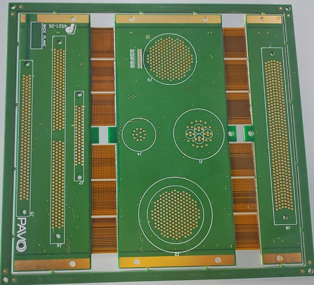
Construction of 20 Layer HDI Boards
The construction of 20 layer HDI boards represents the cutting edge of PCB fabrication technology. Here are some of the key techniques used:
- Build-up Process – The multilayer board is constructed by sequentially laminating dielectric and copper foil layers. This allows the very thin trace spacings and high layer count.
- Microvias – Small vias with 4-6 mil diameters electrically connect traces between layers. The many microvia layers are staggered to maximize interconnect density.
- Thin Dielectrics – Dielectric build-up layers as thin as 2-3 mils separate the thin copper traces. Thicker 8-10 mil cores provide rigidity.
- Laser Drilling – Microvias are typically laser drilled to achieve the small via diameters and precision alignment between layers.
- Fine Line Photolithography – Advanced photolithographic processes pattern extremely fine trace widths and spacings.
- Plating Processes – Electroless and electrolytic copper plating deposits build up trace thickness after patterning.
- Solder Mask and Legend – A solder mask isolates copper traces, while solder pads openings allow component connections. The legend prints identifying nomenclature.
Applications of 20 Layer HDI
The dense interconnectivity of 20 layer HDI boards provides many advantages for cutting-edge electronic devices:
- Smartphones – Accommodate more functionality like cameras, displays, sensors, and processors in the compact form factor.
- Wearables – Facilitate integration of complex flexible circuits in smart watches, fitness trackers, and VR headsets.
- Medical Devices – Enable miniaturized implantables and innovative new surgical tools.
- Automotive Electronics – Help integrate advanced driver assistance systems (ADAS) and infotainment features.
- Aerospace and Defense – Ruggedized electronics for guidance systems, communications, and sensors.
- IoT Devices – Drive the trend toward smaller, smarter internet-connected devices.
As electronic innovation pushes the limits of what is possible in product design, 20 layer HDI provides the interconnect foundation to make it happen.
The Future of HDI Technology
Looking ahead, HDI technology will continue to progress to keep pace with the demands of electronic product development. Here are some potential advances on the horizon:
- Higher Layer Counts – 24, 28, even 32 layer HDI boards for the ultimate in routing density.
- Finer Features – Traces and spaces shrinking below 2 mils to increase interconnects.
- Any-Layer Microvias – Seamless transitions between any layers instead of just adjacent layers.
- Embedded Passives – Burying capacitors and resistors inside the PCB layers.
- Flexible and Rigid-Flex – Incorporating flexible circuits into sections of the HDI board.
- 3D Chip Stacking – Integrating multiple dies stacked vertically using high density interconnects.
- Heterogeneous Integration – Combining dissimilar technologies like silicon, glass, and thin films.
- Additive Manufacturing – 3D printing circuitry with advanced materials and density.
The same technology innovations that are driving the capabilities of 20 layer HDI boards will continue to advance PCB designs to new paradigms.
Frequently Asked Questions
Here are answers to some common questions about 20 layer HDI board technology:
Q: What are the main fabrication challenges with 20 layer HDI boards?
A: Achieving very dense trace spacings, drilling high aspect ratio microvias, and preventing defects across 20 layers of interconnects are some of the key challenges. This requires advanced fabrication tools and extremely tight process control.
Q: Is there a limit to how many HDI layers can be incorporated into a PCB?
A: There are certainly fabrication challenges that increase with higher layer counts. However, constantly evolving technology is enabling further increases in layer count. 32 layers is about the current practical limit, but this will likely advance in the future.
Q: How do you repair or rework 20 layer HDI boards if there is a defect?
A: Repairing defects in multilayer boards is very difficult, especially on inner layers. Often it is more cost-effective to scrap defective boards. High-end inspection systems help improve process yields.
Q: Can flex circuits also be designed with 20 layer HDI technology?
A: Yes, the same build-up processes used for rigid multilayer boards can be applied to create flexible 20 layer HDI circuits. This provides unique advantages for bendable electronics.
Q: What design considerations are important when working with 20 layer HDI boards?
A: Careful layout for signal integrity, thermal management, EMI control, power delivery, and manufacturability is essential. HDI design requires tight collaboration between designers and fabricators.


Leave a Reply