
Introduction
Printed circuit boards (PCBs) are essential components in nearly every electronic device, from smartphones and laptops to industrial equipment and medical devices. As electronic products become smaller and more complex, there is increasing demand for densely-packed PCBs that allow for more electronic components and circuitry in a compact footprint. This is where high-density interconnect (HDI) PCBs become advantageous.
HDI PCBs have emerged as an enabling technology for miniaturization and increased functionality. They utilize finer lines, tighter tolerances, and thinner dielectric materials to achieve a higher circuit density compared to conventional PCBs. HDI techniques allow tracing spacing and via sizes to be reduced to the point where microvia PCBs with trace widths and spacings below 100 microns can be reliably produced.
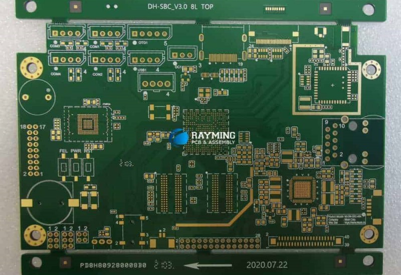
While HDI PCBs traditionally have 4-8 layers, some applications require even higher layer counts up to 18 layers or more. In this article, we will take a deeper look into 18 layer HDI PCB technology and the key considerations for design and manufacturing.
What are 18 Layer HDI PCBs?
An 18 layer HDI PCB contains 18 conductive copper layers that are laminated together with insulating dielectric materials in between each layer. The board will have 18 full conductive layers and 17 dielectric layers.
The layers in an 18 layer board are arranged as follows:
- Top and bottom outer layers (Layer 1 and Layer 18)
- Top and bottom middle layers (Layer 2 and Layer 17)
- Inner layer 1 through inner layer 16
The most common dielectric materials used in HDI boards are polyimide and bismaleimide triazine (BT). These provide the electrical isolation between copper layers and allow for very thin dielectrics down to 12.5 microns or lower. This enables tight spacing of traces and high interconnect density.
Key Characteristics
Some key characteristics of 18 layer HDI PCBs:
- Trace/space and via sizes below 100 microns (2-3x denser than standard PCBs)
- Dielectric layer thicknesses from 12.5 to 50 microns
- High interconnect density >200,000 holes per square meter
- Laser drilled microvias as small as 50 microns
- 1 mil line and space
- Very thin overall board thickness <2.0 mm
- Fine line etching down to 8 microns
Applications
The ultra-high interconnect density and thin profiles of 18 layer HDI PCBs make them well suited for space constrained and miniaturized electronics, such as:
- Smartphones
- Tablets/Laptops
- Medical devices
- Automotive electronics
- Wearables and IoT devices
- Aerospace and avionics
They are especially useful when the product requirements demand small form factors, high processing capabilities, and tight integration of components. The high layer counts provide enough routing channels to accommodate complex circuitry and components.
Benefits of 18 Layer HDI PCBs
There are several key benefits that 18 layer HDI PCBs can provide compared to boards with fewer layers:
Space Savings
The ultra-high interconnect density enables more circuitry and components to fit into a given footprint. This allows for space savings and smaller overall product size.
Routing Capability
With 18 layers, there is more routing capacity to accommodate complex circuit routing on densely packed boards. Sensitive signals can be assigned to inner layers for shielding.
Miniaturization
Components can be packed closer together when trace widths and spaces are reduced. More functionality can fit into a smaller PCB surface area.
Signal Integrity
Careful stackup design along with ultra-short routing enhances signal speed and integrity. This helps maintain signal quality at high frequencies.
Manufacturability
HDI techniques enable reliable production of micro-sized features. Established design rules assure manufacturability.
Cost Reduction
By enabling greater functionality per unit area, 18 layer HDI boards can reduce the overall number of PCBs required in a product. This can lead to reduced materials, assembly, and test costs at the system level.
Challenges with 18 Layer HDI PCBs
While offering advantages, moving to 18 layers also poses some challenges:
Design Complexity
With 18 layers to work with, routing and pin assignment become more complex. This requires experienced PCB designers.
Layer Registration
Precision laser drilling and careful layer-to-layer registration is critical with microvias spanning multiple layers. This requires advanced manufacturing processes.
Testing and Inspection
High density designs make it difficult to probe test points on the PCB surface. Specialized x-ray inspection tools are needed to verify inner layer integrity.
Thermal Management
Densely packed designs can lead to concentrated heat buildup. Thermal analysis and planning for heat dissipation are critical.
EMI Control
Cramming more components and circuitry into a small space increases electromagnetic interference (EMI) risks. Shielding and containment strategies must be incorporated.
Cost
18 layer boards demand advanced manufacturing equipment. They require extensive engineering input. This leads to higher costs compared to simpler PCBs.
HDI PCB Stackup Design and Layout
Stackup design is a very important consideration when working with 18 layer HDI PCBs. The stackup defines the layer configuration, dielectric materials used, and electrical properties between layers. It establishes the foundation for routing high speed signals properly across the board. Some key guidelines for 18 layer stackup design:
- Plan differential pair routing early and assign pairs to adjacent layers to control impedance.
- Use very thin dielectrics between layers to maintain 100 ohm differential impedance with 5/5 mil traces.
- Place ground planes adjacent to outer layers to provide shielding andREFERENCE.
- Ensure power and ground structures have low impedance to handle current demands.
- Alternate signal layers with ground/power layers to isolate signals.
- Assign critical high speed traces to inner layers for shielding.
- Limit the number of lamination cycles to avoid excessive dielectric thickness.
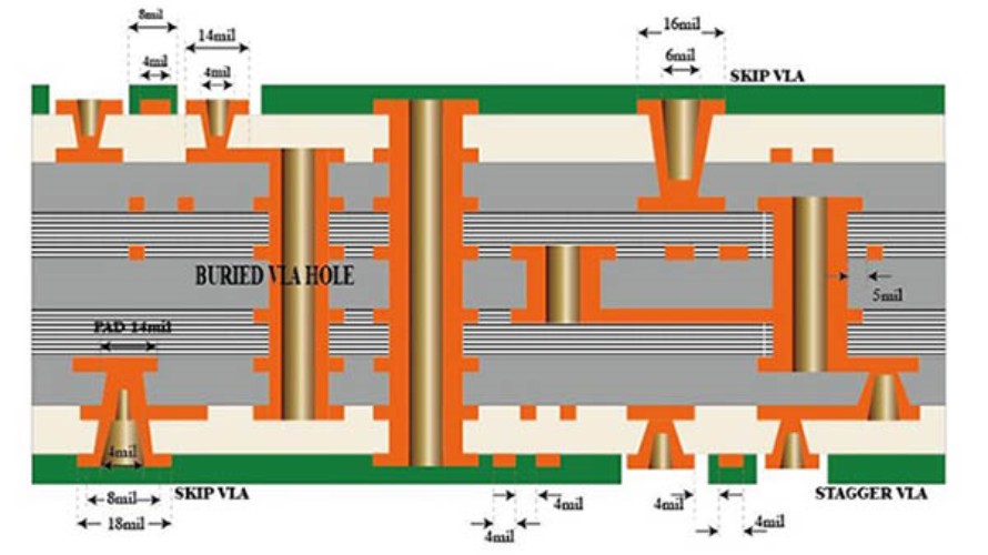
- Allow for 2:1 aspect ratio vias, e.g. 50um laser drilled via with 100um pad.
- Watch out for disproportionate copper distribution between layers which can lead to thermal issues.
In addition to stackup design, HDI layout practices must also be followed:
- Leverage CAD tools with high density design capabilities
- Work with your PCB partner early to define manufacturable design rules
- Use smaller components and fine pitch packaging where possible
- Allow adequate spacing around BGA pads for routing escape points
- Plan routing on inner layers first to relieve congestion on outer layers
- Utilize blind and buried vias to optimize routing across layers
- Incorporate thermal relief structures in large copper shapes
- Include X-Y routing for power and signals to improve impedance control
Key Manufacturing Processes for 18 Layer HDI
Layer Preparation
The core starts with a large panel coated with ultra-thin liquid dielectric material onto which copper foil is laminated. Foil thickness is typically 1⁄2 oz or 1 oz. registration holes aid in aligning layers.
Laser Drilling
A YAG laser drills blind and through-hole vias with diameters as low as 50 microns through multiple dielectric layers with precision registration between layers. Plasma cleansing follows.
Metallization and Plating
PTH holes are seeded and electroplated with copper while blind vias are plated using sputtered copper. Panel surfaces are plated with electroless copper followed by electrolytic copper.
Photolithography
Liquid photo-imageable (LPI) solder mask is applied and exposed to define solder mask openings. Likewise, etch resist LPI defines circuit traces after exposure and development.
Etching
Immersion in ferric chloride etches away unwanted copper to create fine line traces and isolation between traces.
Solder Mask & Legend
The solder mask provides electrical insulation and environmental protection. Silkscreen legend identifies components, testpoints, and board information.
Surface Finish
Immersion silver, ENIG, or OSP coating is applied to protect copper traces from corrosion and prepare for soldering.
Electrical Testing
Continuity, opens, and shorts between traces and testpoints are verified. Automated optical inspection looks for defects and fully tests board connectivity.
Panel Singulation
The panels are depanelized into individual PCBs using routing, scoring, or Breakaway tabs. Visual inspection follows before shipping.
Key Factors in Selecting a PCB Manufacturer
Choosing the right PCB manufacturer is crucial when venturing into advanced HDI boards. Here are some key factors to evaluate:
HDI Experience
Look for extensive experience with volume HDI PCB manufacturing including at high layer counts. Examine their HDI customer base and examples of complex boards previously produced.
Engineering Support
Strong engineering support is essential during design, prototyping, and process qualification. Ask about their design rule development, stackup review, and pre-production engineering services.
Quality Systems
Look for robust quality systems, process controls, and certification such as ISO 9001. Verify they meet industry standards such as IPC-6012 for HDI acceptability. Examine internal quality metrics.
Equipment and Capabilities
Advanced equipment is required including laser drills, photolithography with fine L/S capability, and x-ray inspection. Ensure the facility is geared for high mix, low/medium volume production.
Supply Chain Management
The ability to procure raw materials including specialized laminates is critical to avoiding long lead times. Review their supply chain practices and business continuity provisions.
Cost and Delivery
Factor in total cost including engineering support, prep costs, and associated lead times. Make sure they can deliver prototypes quickly and meet demands of low-medium production runs.
FQA
What are the key benefits of 18 layer HDI PCBs?
Some key benefits of 18 layer HDI PCBs are space savings from higher component density, increased routing capability for complex circuitry, improved signal integrity, and potential cost reduction at the system level. The high layer count provides more channels for routing signals on a compact board area.
What are some typical applications for 18 layer boards?
Typical applications that utilize 18 layer HDI PCBs include smartphones, tablets, laptops, medical devices, automotive electronics, wearables, IoT devices, and aerospace avionics. The boards are useful when space is extremely constrained but high processing capabilities are required.
What are some key challenges with 18 layer HDI boards?
Some key challenges are increased design complexity, layer registration demands, testing difficulties due to high density, thermal management issues, increased EMI risks, and higher overall costs. This requires experienced design resources, advanced manufacturing equipment, and consideration of thermal management early in the process.
What are some critical aspects of the PCB stackup for 18 layers?
Critical aspects of an 18 layer PCB stackup are arranging power and ground layers to control impedance, assigning critical signals to inner layers, using very thin dielectrics, minimizing lamination cycles, sizing components for HDI assembly, allowing for microvia transitions, and watching for uneven copper distribution between layers.
How can you ensure manufacturability when designing 18 layer boards?
Strategies to ensure manufacturability include early engagement with the PCB manufacturer to establish design rules, planning routing on inner layers first, leveraging HDI-capable CAD tools, incorporating thermal relief patterns, utilizing blind/buried vias judiciously, allowing adequate spacing around fine pitch BGAs, and minimizing keypad count variations between layers.


Leave a Reply