
Printed circuit boards (PCBs) are essential components in most electronic devices today. As devices get more complex and pack in more features, the PCBs need to have more layers to accommodate the circuitry and components. 16 layer PCBs allow for highly dense and complex circuit designs for advanced electronics. Selecting the right 16 layer PCB manufacturer is crucial to get high quality boards produced reliably. This article provides a guide on factors to consider when choosing a 16 layer PCB manufacturer and top manufacturers in the industry.
What is a 16 Layer PCB?
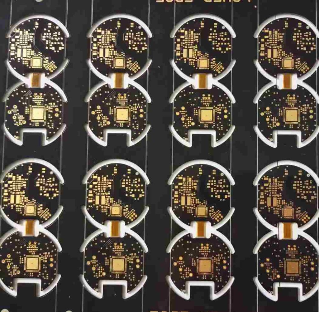
A printed circuit board mechanically supports and electrically connects components using conductive tracks, pads and other features etched from copper sheets laminated onto a non-conductive substrate. PCBs are made up of layers of conductive and non-conductive materials sandwiched together.
The number of layers refers to the number of conductive copper layers in the PCB. 16 layer PCBs contain 16 layers of circuitry to accommodate complex circuit designs. The conductive layers are interleaved with non-conductive dielectric layers for insulation. Vias or plated through holes electrically connect traces between layers.
Benefits of 16 Layer PCBs
- Higher component density: More layers allow fitting more components and circuitry in a compact space. This enables smaller and thinner PCBs ideal for space-constrained electronics.
- Complex circuit routing: With more layers, traces can criss-cross between layers to achieve complex routing not feasible on fewer layer boards. Allows for high speed design.
- Split power planes: Separate power and ground planes can be incorporated to provide clean power distribution.
- RF/high speed design: Additional layers help manage impedance and crosstalk for radio frequency and high speed circuits.
- Noise isolation: Critical signals can be isolated from noise sources by routing them on inner layers.
Applications of 16 Layer PCBs
Some common applications of 16 layer PCBs include:
- High density interconnect (HDI) PCBs for smartphones, tablets and wearables. Allows packing maximum functionality into small form factors.
- Servers, network and telecom hardware with complex circuitry and many components.
- Advanced graphics cards and PC motherboards for gamers and workstations.
- High speed electronic test and measurement equipment.
- Medical equipment like MRI machines, ultrasound scanners.
- Aerospace and defense electronics systems.
- Automotive electronics for ADAS, infotainment systems.
Factors to Consider in a 16 Layer PCB Manufacturer
Choosing the right 16 layer PCB manufacturer is critical to get well-fabricated boards reliably over the product life-cycle. Here are important factors to evaluate potential manufacturers on:
Capabilities
- Technology: Look for manufacturers using latest fabrication processes and equipment. This enables advanced PCBs like 16-36 layer HDI boards, flexible PCBs, rigid-flex boards etc.
- Quality certifications: Key certifications like ISO 9001 and IATF 16949 indicate adherence to quality processes. Some also have AS9100D for aerospace work.
- DFM practices: Design for Manufacturability (DFM) analysis during design validation ensures manufacturability. This avoids costly re-spins later.
- Testing capabilities: Manufacturer should have testing services like flying probe, boundary scan etc. for electrical testing and quality validation.
- Materials used: Assess conductor, dielectric and finishing material options available. FR-4, polyimides, ceramic substrates and more.
- Lead times: See standard and expedited lead times offered. Shorter the better.
- On-time delivery record: Look for >95% on-time delivery rate. Indicates ability to meet schedule commitments.
- Prototyping support: Quick-turn prototype services help test design early at low costs.
- Design support: Having design review services helps improve manufacturability and avoid errors.
- Supply chain management: Look for well-managed supply chains for parts and materials to avoid production delays.
Pricing
- Pricing model: Some offer low unit costs at high volumes while others favor low volume prototyping. See what model fits best.
- Pricing structure: Per PCB area vs. per quantity pricing. Additional costs for features like HAL, blind/buried vias etc.
- Economies of scale: Unit price should drop significantly with order quantity due to optimization of board fabrication.
- Shipping costs: Confirm if shipping/freight costs are included or additional. Domestic vs overseas options.
- Payment terms: Check payment modes accepted and payment terms like advance payment, credit periods etc.
- Tariffs: For overseas manufacturers, be aware of import duties and tariffs that increase overall costs.
Production Capacity
- Output volume: Higher output capacity ensures ability to meet high quantity orders without delays.
- Facilities: Manufacturers should have facilities designed specifically for efficient PCB production.
- Production equipment: Look for multiple SMT lines, automated assembly, test and inspection equipment for faster production.
- Staffing: Well trained staff with expertise in PCB fabrication technologies and processes.
- Scalability: See if they can scale production to handle growing order volumes flexibly. Avoid vendors who are stretched at capacity.
Post Sales Support
- Warranty policy: Warranty period offered on workmanship defects. At least 1 year is common.
- After sales service: Quick issue resolution and excellent technical support.
- Returns/remakes: Ability to get replacements or redo boards if required, though best avoided.
- Cancelation policy: Check if work-in-progress orders can be canceled or modified if needed.
- Documentation: Test reports, certificates of conformity, data packages should be provided.
- UL certification support: Help in getting end product UL certified for safety compliance.
- IP protection: Robust measures to protect intellectual property and avoid counterfeiting.
Top 16 Layer PCB Manufacturers
Here are some of the leading global PCB manufacturers with capabilities to produce high quality, complex 16 layer boards suitable for demanding applications:
Advanced Circuits
Colorado based, with over 25 years of PCB manufacturing experience and ISO 9001:2015 certification. Offers 16-36 layer HDI boards, controlled impedance, blind/buried vias and more. Competitive pricing with domestic US production.
Bittele Electronics
Toronto based manufacturer offering Rigid PCBs, HDI boards, Rigid-flex PCBs and advanced assembly services. Known for quick-turn prototyping.
Eurocircuits
Leading European PCB producer based in Austria with branch offices globally. Specialized in 16-20 layer HDI boards. Can take on highly complex designs.
NCAB Group
Swedish headquartered company with design and production facilities globally including China. A major PCB supplier in Europe, well reputed for high-mix, low to medium volume orders.
PCBCart
Shenzhen based manufacturer focused on high-mix, low volume production. Known for 16-36 layer boards with blind/buried vias, microvias and AL/WL HDI circuits. Affordable prototyping.
PCBWay
China based but ships globally. One of the largest PCB suppliers worldwide. Competitive pricing, efficient production and short lead times.
Sierra Circuits
California based producer supporting rigid, flex, rigid-flex and HDI PCBs. Known for quick-turn and engineering support. ITAR certified and trusted for defense work.
Sunstone Circuits
Oregon based manufacturer popular for prototype and low-medium volume production, including multilayer boards. Provides helpful online DFM analysis.
Ray PCB Solutions
Chinese manufacturer focused on high density interconnect PCBs including up to 36 layers. Well suited for advanced electronics and fast turnaround.
Unimicron
Major Taiwan based PCB provider with large facilities globally. High reliability rigid, flex, HDI boards for automotive, telecom industries.
Würth Elektronik eiSos
German PCB manufacturer that is part of the Würth Elektronik Group. Produces technologically advanced circuit carriers.
How to Get the Best Results from 16 Layer PCB Manufacturers?
Follow these tips to ensure you get the most successful outcome when ordering 16 layer PCBs:
- Engage the manufacturer early in the design phase for design reviews and DFM analysis. This optimizes the design for manufacturability.
- Provide complete design information – complete schematics, bill of materials, layer stackup, finished copper, solder masks etc. Ensure your design files/Gerbers adhere to requirements.
- Leave adequate tolerances for conductor widths, annular rings, drill sizes, spacing between traces etc. as per IPC standards. Tighter tolerances increase cost.
- Use a consistent coordinate system on all layers to avoid misalignment. Have clear layer registration markings.
- Avoid via-in-pad as much as possible. Use blind/buried vias instead of through hole vias for dense HDI stacking.
- Watch out for impedance discontinuities at layer transitions which cause reflections in high speed transmission lines.
- Include test points for validation during manufacturing and for end-product testing.
- Specify quality requirements clearly – IPC class 2 and 3 are common for high reliability.
- Order PCB samples first to check quality before full production run.
- Get test reports from the manufacturer to validate electrical functioning.
- Have backups in your supply chain to account for uncertainties in delivery.
Frequently Asked Questions
What are some challenges in manufacturing 16 layer PCBs?
Some manufacturing challenges are:
- Achieving tight registration between layers – +/- 0.1mm tolerance
- Getting good via and hole wall quality due to high aspect ratios
- Controlling impedances accurately across layer transitions
- Fabricating boards without any faults – specs require <1% shorts
- Solder mask curing when coating inner layers
- Thermal management across the thickness during lamination
What are the typical lead times for 16 layer PCBs?
Typical lead times are:
- Prototypes: 3-7 days
- Small volumes <50 pcs: 15-20 days
- Medium volumes <500 pcs: 20-25 days
- High volumes >500 pcs: 25-30 days
Leading manufacturers can often ship quicker. Lead times also depend on order backlogs.
What design software do professionals use for 16 layer PCBs?
Popular PCB design software packages are:
- Altium Designer
- Cadence Allegro and OrCAD
- Mentor Graphics Xpedition
- Zuken CR-8000
- Pads from Siemens EDA
- Eagle from Autodesk
Altium and Cadence tools are most common among PCB designers.
What are the typical costs for 2-layer vs 16-layer PCBs?
As a rough estimate for small quantities of simple boards:
- 2-layer PCBs: $100 – $500
- 16-layer HDI PCBs: $2000 – $5000
Costs vary significantly based on complexity, order volume, lead time etc. HDI PCBs with micro-vias are more expensive.
How are defects reduced in multi-layer PCB fabrication?
Common methods to improve 16-layer PCB quality are:
- Automated optical inspection (AOI) after each production step
- Testing laminate quality before pressing
- Careful drilling with optimized parameters to avoid drill smearing
- Plasma etching to clean drill holes and improve connections
- Elemental analysis of copper to ensure high purity
- Improved registration techniques for aligning layers
- Use of liquid photoimageable solder masks (LPISM)


Leave a Reply