Introduction
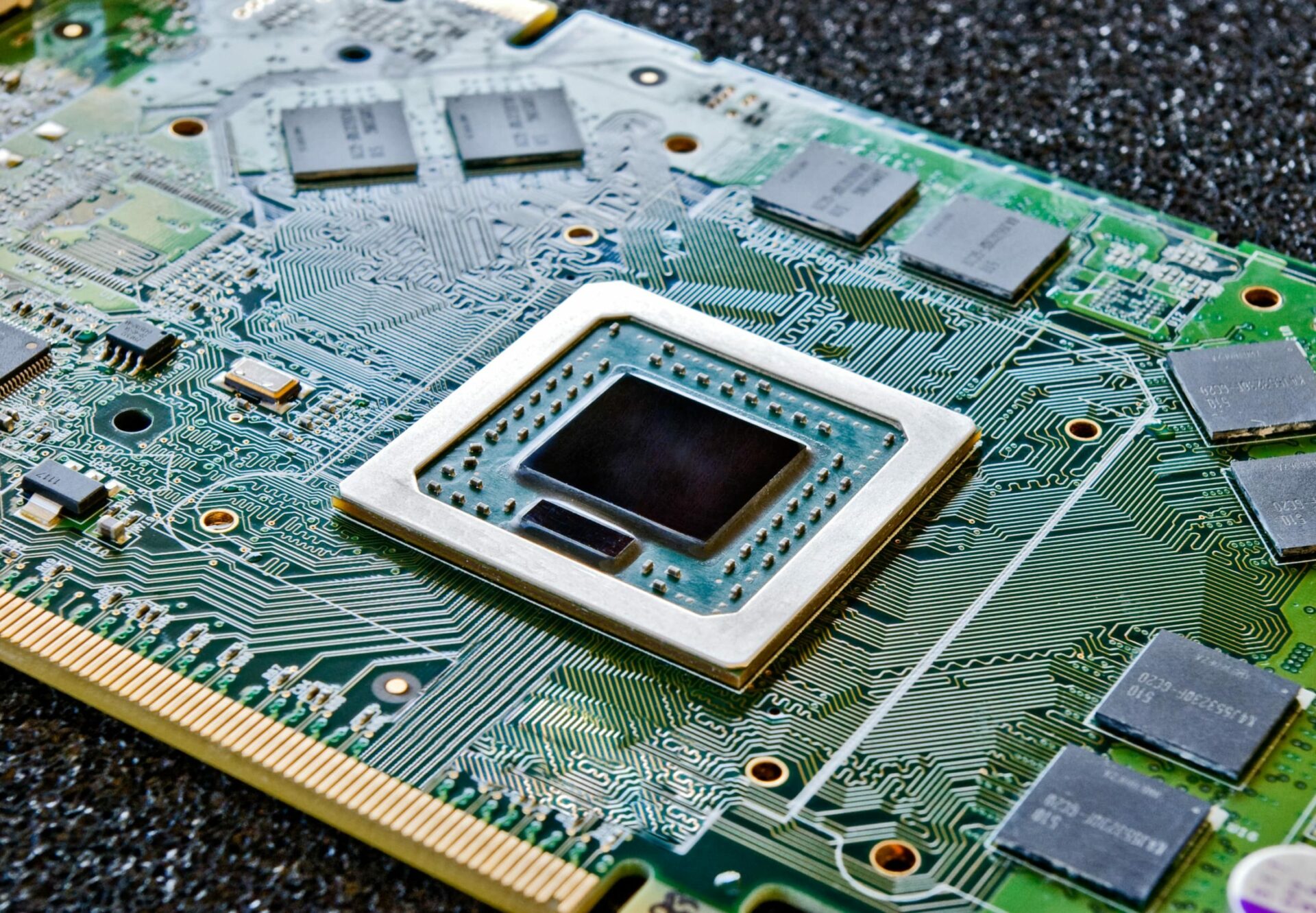
A 16 layer high density interconnect (HDI) printed circuit board (PCB) contains 16 layers of circuitry sandwiched together. HDI PCBs enable innovative and complex designs by packing more interconnects into a smaller space. They are used for products that require high speed, high frequency or high density circuitry like electronics, telecommunications equipment, aerospace and defense systems.
With the right design and manufacturing process, 16 layer HDI PCBs provide several benefits:
- Higher interconnect density for more complex circuitry
- Miniaturization of products
- Improved electrical performance
- Higher speeds and frequencies
- More efficient routing
- Better signal integrity
- Lower noise and crosstalk
However, designing and producing quality 16 layer HDI PCBs requires expertise. This article will provide a technical overview of 16 layer HDI PCB technology, discuss design considerations, and outline the manufacturing process.
HDI PCB Technology

HDI stands for high density interconnect. This refers to the use of microvias to connect layers in a PCB.
Microvias are small vias with diameters less than 150 microns (0.006 inches). Regular plated through hole (PTH) vias have larger diameters, typically above 250 microns.
By using laser drilling, microvias can have very tight spacing, allowing routing between layers in an area that would only support a single large via. This enables greater vertical connectivity.
In addition to microvias, HDI PCBs also utilize thinner dielectric buildup layers, typically around 25-50 microns. The resulting structures allow placing traces closer together and embedding passive components like resistors and capacitors.
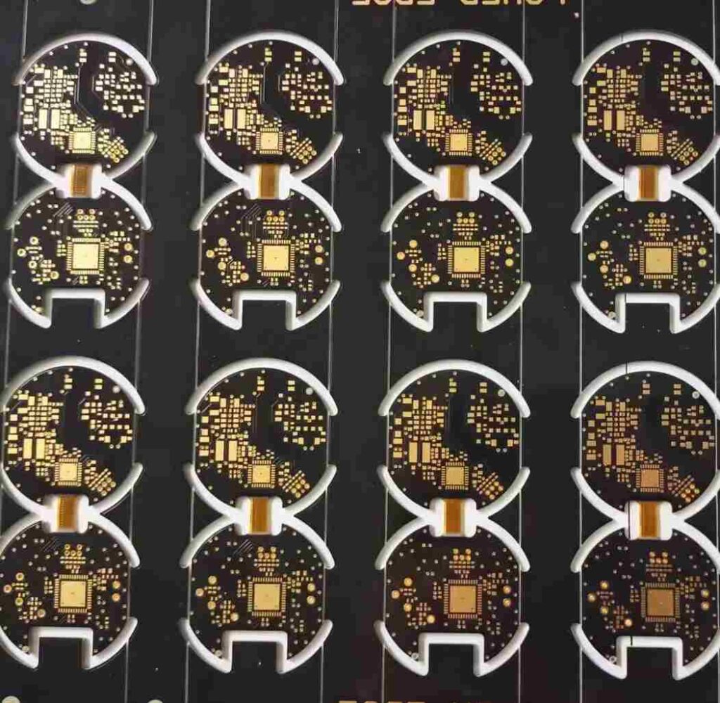
16 layer HDI designs utilize multiple HDI sub-structures:
- Core: The basic foundation, typically a thicker PCB material with lower density interconnects. Provides mechanical stability.
- Buildup layers: Thinner insulating dielectric layers applied on the core, interleaved with patterned copper layers. This is where the HDI technology enables high density routing.
- Microvias: Small vias drilled with laser and plated to connect the buildup layers. Allows greater vertical connectivity.
- Buried vias: Large vias connecting between buildup layer sections, through the core layer. Provides connectivity between HDI sections.
- Solder mask: Layer of epoxy that protects the outer copper layers from oxidation and prevents solder bridging.
- Silkscreen: Printed layer for markings like part numbers and logos.
This combination of technologies allows extremely complex routing arrangements over 16 layers, enabling far greater circuit density.
16 Layer HDI PCB Design Considerations
Designing a 16 layer HDI PCB requires careful planning and engineering. Here are some key design considerations:
Layer Stackup
Determining the right layer stackup is critical. This refers to the sequence of dielectric, copper and core layers. The stackup impacts trace impedances, crosstalk, signal integrity and manufacturability.
Typical arrangements utilize multiple 4-layer HDI sections connected through the core with buried vias. But this can vary based on design needs. Simulation and analysis tools like HyperLynx can help optimize the stackup.
Routing Channels
With 16 layers, determining routing channels is vital. Groups of layers may be dedicated to power delivery, ground planes, shielding, high speed signals, etc. The channels help isolate circuits with differing requirements.
Tight geometric controls are needed to implement dense HDI routing channels. This is where specialized PCB layout tools become very beneficial.
Via Design
Via design and adjacency is critical for 16 layer HDI PCBs. Microvia capture pads, antipad sizes, stub lengths and other parameters require careful control.Simulation tools can help determine ideal via designs before layout.
Impedance Control
With 16 layers, maintaining tight impedance control is challenging but vital for signal integrity. This requires tightly constrained dielectric thicknesses, trace geometries, laminate selection and fabrication process controls.
Thermal Management
The high circuit density generates significant heat. Careful thermal analysis should be conducted to determine necessary heat dissipation features like thermal vias, ground planes and copper balancing. This helps prevent hot spots.
Power Integrity
Managing voltage drops and DC power delivery can also be difficult with complex 16 layer designs. Planning power supply partitioning, decoupling capacitors and power plane design from the start helps maintain power integrity.
DFM Practices
Following design for manufacturing (DFM) guidelines ensures the 16 layer HDI PCB can be fabricated reliably. Utilizing standard layer arrangements, minimizing via aspect ratios, and designing within tolerances facilitates manufacturability.
16 Layer HDI PCB Manufacturing Process
Producing a high quality, functional 16 layer HDI PCB requires advanced manufacturing capabilities and tight process controls. Here is a brief overview of the complex fabrication process:
Imaging
The design layout data generates photomasks for each layer. Advanced laser mask imaging with 5-20 micron geometries enables very dense patterning.
Core Preparation
Core materials are conditioned through baking, cleaning, surface treatments and drilling to prepare for lamination. Exact process controls prevent deformation.
Layer Lamination
Dielectrics and copper foils are precisely laminated to build up the designed 16 layer stackup arrangement. This utilizes high accuracy mechanical, thermal and pressure controls.
Via Formation
Microvias and through holes are drilled with advanced laser and mechanical drills. High precision hole wall roughness and diameter controls enable reliable plating.
Metallization
Surfaces are pre-treated and seeded to enable uniform electroplating of copper and hole walls. This electrically connects layers according to the layout.
Outer Layer Imaging
Additional photolithography forms the fine line traces and spaces on the outer circuit layers according to the layout.
Solder Mask & Silkscreen
Liquids coatings are applied and imaged to form the solder mask and silkscreen. Tight alignment precision is necessary.
Surface Finishes
Surfaces are plated with ENIG (gold) or other finishes. This protects copper traces from oxidation and enables reliable soldering.
Panel Singulation
The panel is mechanically routed and depanelized into individual PCBs without causing defects. Automated optical inspection checks for any issues.
Testing
Each PCB undergoes electrical testing and quality inspection per IPC standards to ensure proper function and reliability.
This entire process must be conducted within extremely tight standards to produce a high yield of working 16 layer HDI PCBs. Each step leverages advanced fabrication technologies and techniques for precision patterning, lamination, via formation and metallization.
FQA
What are the main benefits of a 16 layer HDI PCB?
The main benefits are higher interconnect density for complex circuitry, improved electrical performance, higher speeds, more efficient routing, better signal integrity, and miniaturization of end products.
What are some key design considerations for 16 layer HDI PCBs?
Critical design considerations include layer stackup, routing channels, via design, impedance control, thermal management, power integrity, and following DFM guidelines.
How are microvias formed in HDI PCBs?
Microvias are formed by laser drilling holes less than 150 microns in diameter through the thin dielectric buildup layers. The holes are then plated with copper to electrically connect the layers.
What fabrication processes are critical for HDI PCBs?
Critical processes include precise imaging, lamination, laser drilling, electroplating, photolithography of outer layers, and testing. Each process requires advanced technologies and tight controls to enable HDI structures.
Why can 16 layer HDI PCBs support higher speeds and frequencies?
The thin dielectric layers reduce capacitance between traces. Shorter routing paths minimize inductance. This allows signals to propagate faster with less loss and distortion.


Leave a Reply