Introduction to 14 Layer HDI PCBs
A 14 layer high density interconnect (HDI) printed circuit board (PCB) is a type of multilayer PCB that contains 14 conductive copper layers laminated together. HDI PCBs have very fine lines and spaces, allowing for higher interconnect density compared to standard PCBs. The 14 layers alternate between signal layers and ground or power planes. The increased number of layers provides more routing channels for signals, reducing the need for vias and allowing for higher component densities.
Some key features of 14 layer HDI PCBs:
- Extremely high wiring density with traces and spaces under 8 mils
- Minimum hole size of 4 to 6 mils
- Stacked microvias with diameters under 6 mils
- Thin dielectric materials between layers (3 to 5 mils)
- Tight impedance control (±5%)
- More signal layers than power/ground layers
14 layer HDI PCBs are used in advanced electronics applications that require miniaturization, high speeds, and complex functionality. The main applications include:
Smartphones and Tablets
The compact form factors of mobile devices require PCBs with very high interconnect density. 14 layer HDI PCBs allow packing more features and connectivity into the limited space.
Servers and Data Center Equipment
Servers demand high speed signaling for fast data transmission. The additional layers in 14 layer HDI PCBs provide more routing channels to maintain signal integrity at multi-gigabit speeds.
Automotive Electronics
Automotive applications need electronics that can withstand vibration, shock, and temperature extremes. The tightly stacked layers and microvias in 14 layer HDI PCBs provide excellent mechanical stability.
Aerospace and Defense Electronics
Ruggedized electronics for aerospace and military use often require miniaturization. 14 layer HDI PCBs allow for smaller, lighter circuitry with proven durability.
Benefits of 14 Layer HDI PCBs
The key benefits that 14 layer HDI PCBs provide compared to standard multilayer PCBs:
Higher Interconnect Density
The thin dielectric layers and fine lines/spaces allow fitting more traces in the same area for maximum interconnect density. This enables miniaturization and integration.
More Routing Channels
14 layers give more routing channels for traces, reducing the need for vias. This improves signal integrity at high speeds.
Smaller Overall Size
More component density and thinner dielectric layers reduce the total PCB thickness. This allows smaller and lighter end products.
Lower System Cost
Higher density reduces the number of PCBs required. Smaller PCB size also lowers materials cost. Overall system cost is reduced.
Better High Speed Performance
Controlled impedances, lower capacitance, and reduced vias help maintain signal integrity at multi-gigabit data rates.
Improved Reliability
The fine features withstand shock, vibration, and flexing. Microvias offer redundancy and eliminate drilling issues.
Enhanced Manufacturability
14 layer HDI PCBs leverage established manufacturing processes for consistent quality and yields.
Challenges with 14 Layer HDI PCBs
While offering significant benefits, designing and manufacturing 14 layer HDI PCBs also poses some challenges:
Tight Tolerances
The small features and thin dielectric layers require very tight tolerances. This demands precise process controls.
Limited Fab Capability
Only high-end PCB fabricators have equipment capable of producing 14 layer HDI boards efficiently.
Complex DFM Rules
Rigorous design for manufacturing (DFM) rules must be followed to avoid problems during production.
Intensive Simulation
Extensive signal and power integrity simulations are needed to verify performance due to minimal design margins.
Thermal Management
The dense, multilayer construction requires careful thermal design to dissipate heat. This often necessitates additional metal core layers.
High Cost
14 layer HDI PCBs have higher fabrication and component assembly costs compared to standard multilayer boards.
However, the technical advantages of 14 layer HDI PCBs outweigh these challenges in most high performance applications.
Design Guidelines for 14 Layer HDI PCBs
To leverage the full benefits of a 14 layer HDI PCB while mitigating the risks, designers should follow these guidelines:
- Work closely with your PCB fabricator during design to ensure manufacturability. Get their input on critical tolerances for line widths, hole sizes, registration, and stackup.
- Use a minimum finished hole size of 4 to 6 mils for microvias. For buried and blind vias, allow 6 to 8 mil finished hole sizes.
- Maintain at least 3 to 5 mils spacing between microvias. Ensure sufficient annular rings based on hole size.
- Restrict microvia aspect ratios to under 1:1. Use stacked microvias when going through multiple layers.
- Hold trace width to 5 mils minimum and 8 mils minimum spacing. Support 6 mil lines and spaces if required.
- Use thinner 1 to 2 oz copper to enable fine features. Heavier copper is difficult to etch.
- Minimize the number of different dielectrics used. This avoids issues with lamination and Z-axis CTE mismatches.
- Include fine pitch components with 6 mil pitch or less. Avoid larger pitch BGAs and connectors.
- Incorporate wirebonding, flip chip, or other advanced assembly if needed to utilize the full substrate density.
- Pay special attention to power integrity. Use multiple power and ground pairs. Do extensive modeling of PDN.
- Simulate high speed channels to control impedance, crosstalk, reflections. Add ground vias next to signals if needed.
By following these guidelines, PCB designers can fully leverage a 14 layer HDI stackup for maximum density, performance, and reliability.
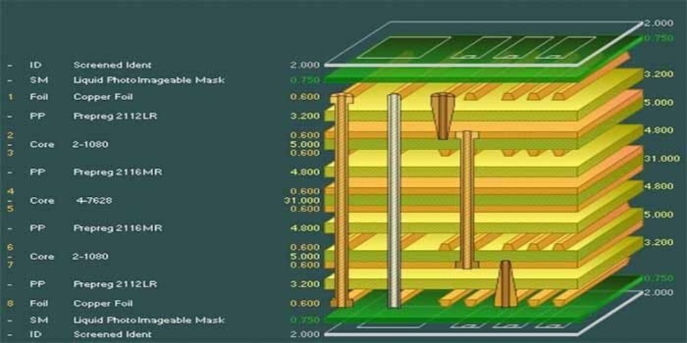
Example 14 Layer HDI PCB Stackup
Here is an example 14 layer HDI PCB stackup with key design details:
| Layer | Layer Type | Thickness | Copper Weight | Dielectric Material | Notes |
|---|---|---|---|---|---|
| 1 | Signal | variable | 1 oz | Liquid Photoimageable Solder Mask | Outer layer 1 |
| 2 | Plane | variable | 1 oz | Isola 370HR | Ground plane 1 |
| 3 | Signal | variable | 1 oz | Isola 370HR | High speed signals |
| 4 | Plane | 3.8 mils | 1 oz | Isola 370HR | Ground plane 2 |
| 5 | Signal | 3.8 mils | 1 oz | Isola 370HR | High speed signals |
| 6 | Plane | 3.8 mils | 1 oz | Isola 370HR | Power plane 1 |
| 7 | Signal | 3.8 mils | 1 oz | Isola 370HR | High speed signals |
| 8 | Plane | 3.8 mils | 1 oz | Isola 370HR | Ground plane 3 |
| 9 | Signal | 3.8 mils | 1 oz | Isola 370HR | High speed signals |
| 10 | Plane | 3.8 mils | 1 oz | Isola 370HR | Power plane 2 |
| 11 | Signal | 3.8 mils | 1 oz | Isola 370HR | High speed signals |
| 12 | Plane | 3.8 mils | 1 oz | Isola 370HR | Ground plane 4 |
| 13 | Signal | 3.8 mils | 1 oz | Isola 370HR | High speed signals |
| 14 | Plane | variable | 1 oz | Isola 370HR | Ground plane 5 |
| 15 | Signal | variable | 1 oz | Liquid Photoimageable Solder Mask | Outer layer 2 |
This stackup uses the high performance Isola 370HR dielectric material for all layers. The core thickness is 3.8 mils per layer to maximize layer count in the minimum overall thickness. 1 oz copper is used to enable fine 5 mil traces and spaces. Microvias with 4 to 6 mil finished diameters are plated through the entire stackup to connect layers. The many ground plane layers isolate the critical high speed signals for improved signal integrity.
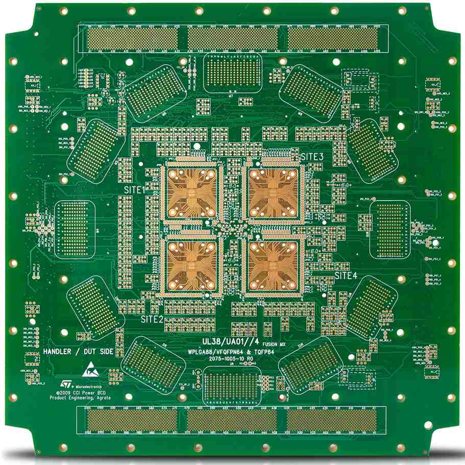
Applications Example: 14 Layer HDI PCB for Smartphone AP
As an example application, here is how a 14 layer HDI PCB can be optimized for a smartphone application processor (AP):
Challenges
- Extremely small form factor
- High computing performance requires multi-GHz speeds
- Thermal output up to 5W
- Withstand drop/shock reliability requirements
- High pin count package (over 1000 I/Os)
PCB Solution
- 14 layer HDI PCB, 60 x 45 mm size
- 4 mil lines/spaces for maximum routing density
- Stacked microvias, 6/6/6/8 configuration
- 4 oz copper inner layers, 2 oz outer layers
- 40μm line width control for impedance matching
- Fine pitch peripheral BGA routing
- Embedded resistor/capacitor layers for decoupling
- Thermal vias under AP for conduction to case
This 14 layer HDI PCB design minimizes the footprint while providing over 25 GB/s serial lane routing performance. The high density interconnects support the advanced AP functionality while meeting the thermal and reliability requirements.
Summary of Key Benefits
To summarize, the key benefits of migrating to a 14 layer HDI PCB include:
- Enable further miniaturization of products
- Pack more electronic functionality into small form factors
- Improve routing for high speed signals up to 50+ Gbps
- Allow increased component densities with fine pitch devices
- Optimize power distribution with multiple power planes
- Reduce system cost through integration and smaller PCB sizes
- Achieve overall performance gains through design optimization
For advanced electronic systems, partnering with a reliable HDI PCB manufacturer can help realize these benefits through the optimal use of a 14 layer PCB platform.
Frequently Asked Questions
What are some typical design rules for 14 layer HDI PCBs?
Typical design rules include:
- Line width/space: 4-8 mils
- Microvia diameter: 4-6 mils
- Microvia pad size: 8-12 mils depending on hole size
- Microvia spacing: 6-8 mils
- Trace width control: ±5% or less
- Dielectric thickness: 3-5 mils
What materials are commonly used?
Isola 370HR, Nelco 4000-13, Rogers RO4350 are popular dielectric materials. 1 oz copper foils are typical for traces. Microvia fills can use either copper or conductive pastes.
How many HDI layers can be stacked together?
Technically over 20 layers is possible, but 14-16 layers is currently the practical limit before fabricability and yield issues arise. Stacked microvias help interconnect the layers reliably.
What are some key steps in manufacturing 14 layer HDI PCBs?
Critical steps include laser drilling microvias, aligning layers with very tight tolerances, filling blind/buried vias, and ensuring thin dielectrics do not get damaged during lamination. Testing for opens/shorts is also essential.
What design tools are recommended?
Use PCB layout tools with support for HDI stackups, microvias, and high speed constraints. For analysis, utilize signal/power integrity and thermal modeling tools to simulate performance.


Leave a Reply