An In-Depth Look at Multi-Layer PCB Technology
Printed circuit boards (PCBs) are essential components in nearly all modern electronics. As devices become more complex and packed with features, PCBs must evolve to accommodate more complicated circuitry and components. This has led to the development of multilayer PCBs with 6, 8, 10 or more conductive layers to allow for greater circuit density and flexibility in routing signals between components.
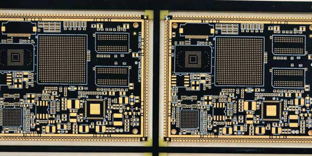
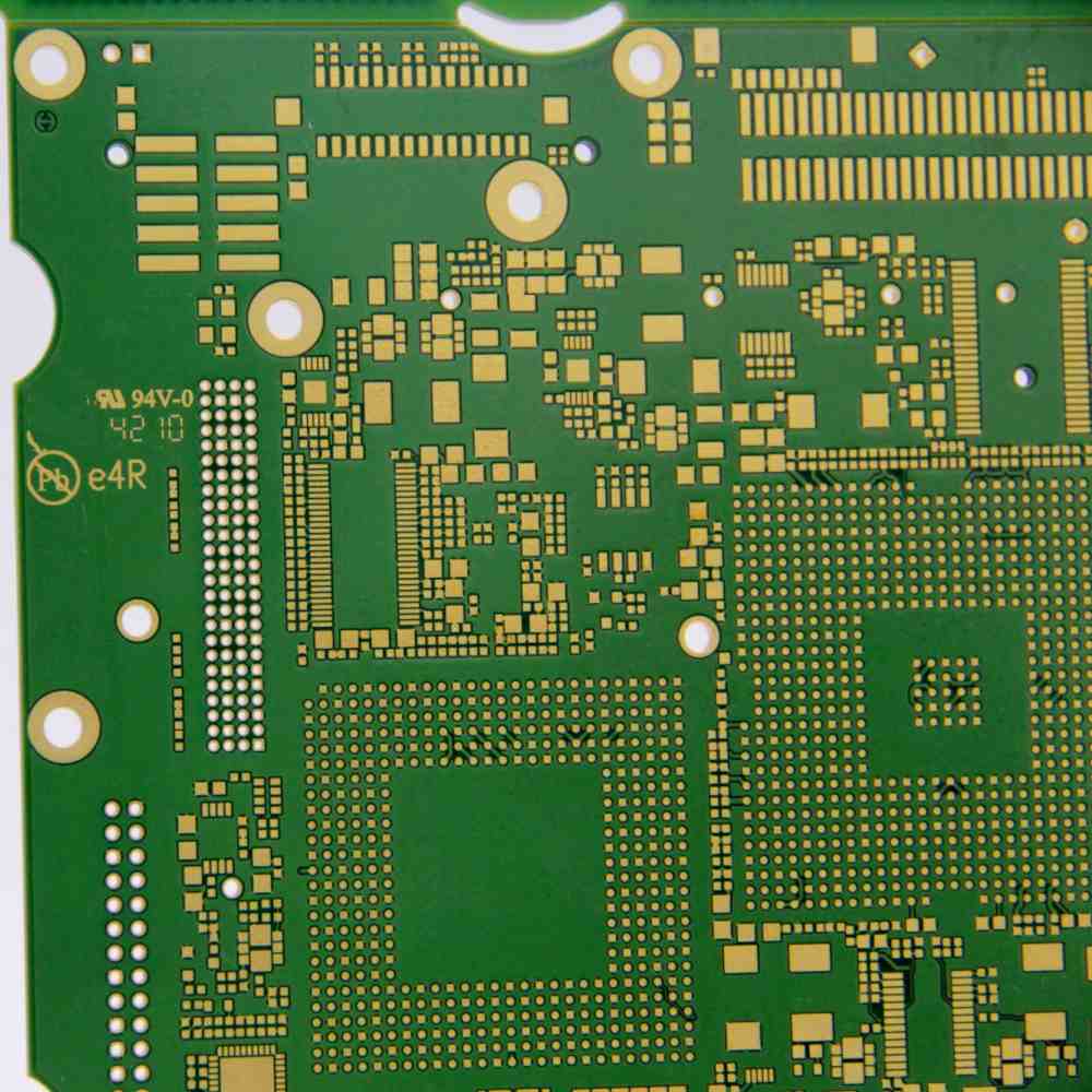
One of the more advanced types of multilayer PCBs is the 12 layer blind buried PCB. These boards provide even more routing capability by embedding conductive layers within the PCB stackup. This article takes an in-depth look at 12 layer blind buried PCB technology and its advantages.
What is a 12 Layer Blind Buried PCB?
A 12 layer PCB contains 12 conductive copper layers that are laminated together with insulating dielectric material. Vias and plated through holes electrically connect traces between layers. Here are some key characteristics of a 12 layer blind buried PCB:
- 12 Total Layers – There are 12 conductive copper layers labeled L1 to L12
- 4 Blind Layers – Layers L2, L3, L10, and L11 are blind layers that do not extend to the outer surfaces of the PCB.
- 4 Buried Layers – Layers L5, L6, L7 and L8 are buried layers sandwiched between other layers.
- Greater Routing Capability – With 12 layers, more routing channels are available for laying out complex circuitry.
- Improved Signal Integrity – Blind and buried layers shield signals from noise. Differential pairs can be routed together.
- Component Density – More layers allows components and vias to be placed close together without interference.
This diagram shows a cross-section of a typical 12 layer blind buried PCB stackup:
| Layer | Type |
|---|---|
| L1 | Signal |
| L2 | Blind |
| L3 | Blind |
| L4 | Signal |
| L5 | Buried |
| L6 | Buried |
| L7 | Buried |
| L8 | Buried |
| L9 | Signal |
| L10 | Blind |
| L11 | Blind |
| L12 | Signal |
Manufacturing Process

Constructing a multilayer PCB with blind and buried layers requires an advanced manufacturing process. Here are the key steps:
- Layup – Sheets of copper foil are stacked up with layers of dielectric prepreg material. The blind and buried layers are inserted within the stackup in their designated positions.
- Lamination – The entire stack is laminated together under heat and pressure. The dielectric material bonds the layers together.
- Drilling – Small holes are drilled through the laminated stack to create the vias. A CNC laser driller is typically used.
- Plating – The walls of the vias are plated with copper to electrically connect traces between layers.
- Etching – Photolithographic processes are used to subtractively etch away copper to form the traces and pads on each layer.
- Solder mask and silkscreen – A solder mask insulates the exposed copper surfaces. Silkscreen provides component legends and branding.
The blind and buried layers require additional steps of laser micro-machining to create access points for drilling vias to these embedded layers.
Benefits of 12 Layer Blind Buried PCBs
Here are some of the major benefits that 12 layer blind buried PCBs provide:
- Increased routing channels – With 12 layers, complex designs with many signals and components can be routed efficiently. The additional blind and buried layers essentially double the routing space compared to a standard 6 layer board.
- Flexibility – Blind and buried layers with planned access points allow routing channels to be utilized wherever needed, not just on the outer layers. Vias can connect traces across multiple layers.
- Signal integrity – Blind and buried layers are shielded within the board stackup. This allows sensitive signals like high-speed data lines and clock signals to be isolated and routed with minimal interference or crosstalk. Differential pair signals can be routed in close proximity.
- Noise isolation – Digital and analog signals can be separated onto different buried layers to keep noise from impacting sensitive analog traces. Grounds and power planes can be embedded between active layers.
- High component density – More PCB layers allows components to be placed very close together without worries of clearance space needed between parts. Vias can also be placed close together thanks to the additional routing layers.
- Miniaturization – By packing more functionality into a smaller PCB area, multilayer boards allow for smaller and more compact end products.
- Mixed signal circuits – Digital, analog and RF circuits can co-exist on one board with signals isolated in their own domains. This removes the need for multiple PCB assemblies.
In summary, 12 layer blind buried PCBs enable highly dense, high performance circuit designs for advanced electronic devices and systems. The tradeoff is increased cost and complexity versus standard 6 or 8 layer PCBs.
Applications of 12 Layer PCBs
Here are some examples of products that utilize 12 layer blind and buried PCBs:
- Smartphones – The latest smartphone designs require 12 layers to interconnect the application processor, memory modules, wireless radios, touchscreen controller, power management ICs, and other components.
- Graphics cards – High speed GPUs, lots of memory, and fast interconnects need 12 layers for routing. Some advanced cards use PCBs with as many as 24 layers.
- Computer servers – Servers need to make high number of reliable connections for processors, memory modules and add-on cards. Complex 12+ layer boards are common.
- Automotive electronics – ADAS systems, infotainment controllers and engine control units in modern vehicles use 12 layer boards to connect myriad sensors.
- Aerospace and defense – Mission computers, flight control systems, radar and communications equipment operate in confined spaces. Multi-layer boards are ideal.
- Medical devices – Hearing aids, implantable devices and diagnostic systems using mixed signal ICs take advantage of multilayer PCB technology.
Almost any advanced electronic product can potentially benefit from the increased routing density and signal isolation of a 12 layer blind/buried PCB. The PCB design itself takes on greater importance to fully utilize the capabilities.
Design Considerations
Here are some key considerations when designing a 12 layer blind buried PCB:
Layer Stackup – The stackup must be carefully planned out based on the types of signals being routed and how components need to interconnect. Critical clocks and high speed traces require layers with good isolation from noise sources.
Split Planes vs. Solid Planes – Split power or ground planes allow segments to be powered on/off for better control. Solid planes provide the best noise shielding. Mix split and solid planes as needed.
Blind/Buried Access – Microvias need to be planned to bring signals up/down to blind/buried layers. Groups of microvias can serve as access points to buried layers if signals are clustered.
Impedance Control – Trace width and spacing must be controlled so traces have proper impedance for match transmission lines, high speed signals, and differential pairs.
Plane JUMPERS – Jumper connections may be needed between split plane segments to reduce impedance discontinuities. But jumpers can also allow more noise coupling, so use judiciously.
Component Placement – Ensure components have access to their needed signals and power/ground layers. Watch length of sensitive traces. Verify components fit board dimensions.
Thermal Management – More layers restrict heat transfer through the PCB. Thermal vias, copper fills, exposed pads and other cooling methods help mitigate this.
Manufacturing Limitations – Work with your PCB fabricator to ensure your design adheres to their process capabilities for hole sizes, trace space/width, aspect ratios, etc.
A disciplined approach to layer planning, schematic capture, and PCB layout is essential to utilizing 12 layers effectively while avoiding issues like signal interference or high stub resonances. Simulation and prototyping should be used to verify performance before full production.
FAQ
Here are answers to some frequently asked questions about 12 layer blind buried PCBs:
Q: How much more does a 12 layer PCB cost versus a standard 6 layer board?
A: In general, each additional conductive layer adds cost, complexity, and lead time to a PCB. A 12 layer board would typically cost at least twice as much as an equivalent 6 layer design. Actual pricing depends on pcb quantity and fabrication factors.
Q: Can all 12 layers be used for routing signals?
A: Not usually. It’s common to reserve the inner layers for ground and power planes. So in practice, only L1, L4, L9 and L12 might be used for critical signals requiring isolation from other layers.
Q: What are the disadvantages of using a 12 layer board?
A: Mainly increased cost and manufacturing lead times. Thermal performance is reduced, potentially requiring heatsinks or thermal vias. High layer counts also increase the risk of defects occurring.
Q: How small can the microvias be to access a buried layer?
A: Laser drilled microvias allow connections to buried layers with via pads as small as 0.15mm. This supports very high interconnect density. Mechanical PTH drilling typically limits minimum via size to 0.20-0.25mm.
Q: Can RF circuits be integrated onto 12 layer boards?
A: Yes, RF traces and components can potentially be isolated on specific layers. Impedance control and preventing unwanted coupling are major considerations for RF layout.
So in summary, 12 layer blind and buried PCBs enable highly complex routing for advanced circuits and systems. The tradeoff is increased cost and design effort, which must be weighed against performance benefits. When designed properly, 12+ layer PCBs bring powerful advantages for routing density, signal integrity and noise isolation in leading-edge electronic devices.


Leave a Reply